2 layers125 × 125 mm

 ArgonautGit/wallet_dmm
A multimeter the size of a credit card: DC volts, resistance, continuity and diode test, shown on a 0.91" OLED, with three buttons, an RGB LED and a piezo beeper.
Wallet dmm is an open-source printed circuit board by ArgonautGit, from the ArgonautGit/wallet_dmm repository on GitHub. It is a 2-layer board of 85.6 × 54 mm with 70 parts on 58 nets, routed with 499 tracks and 147 vias.
It is built around the STM32L051K8T6, MCP73831T-2ACI/OT-HXY and TL431AIDBZR, with the XC6206P302MR-G, CC0603KRX7R9BB104 and BAV199,215-JSM among its other parts. Its parts include 30 resistors, 14 capacitors, 5 connectors, 5 switches and 4 ICs. It belongs with the STM32 boards of this library.


A multimeter the size of a credit card: DC volts, resistance, continuity and diode test, shown on a 0.91" OLED, with three buttons, an RGB LED and a piezo beeper. It runs from a small LiPo that charges over USB-C and is built around an STM32L051K8, with Rust firmware and a simulation of the whole thing.
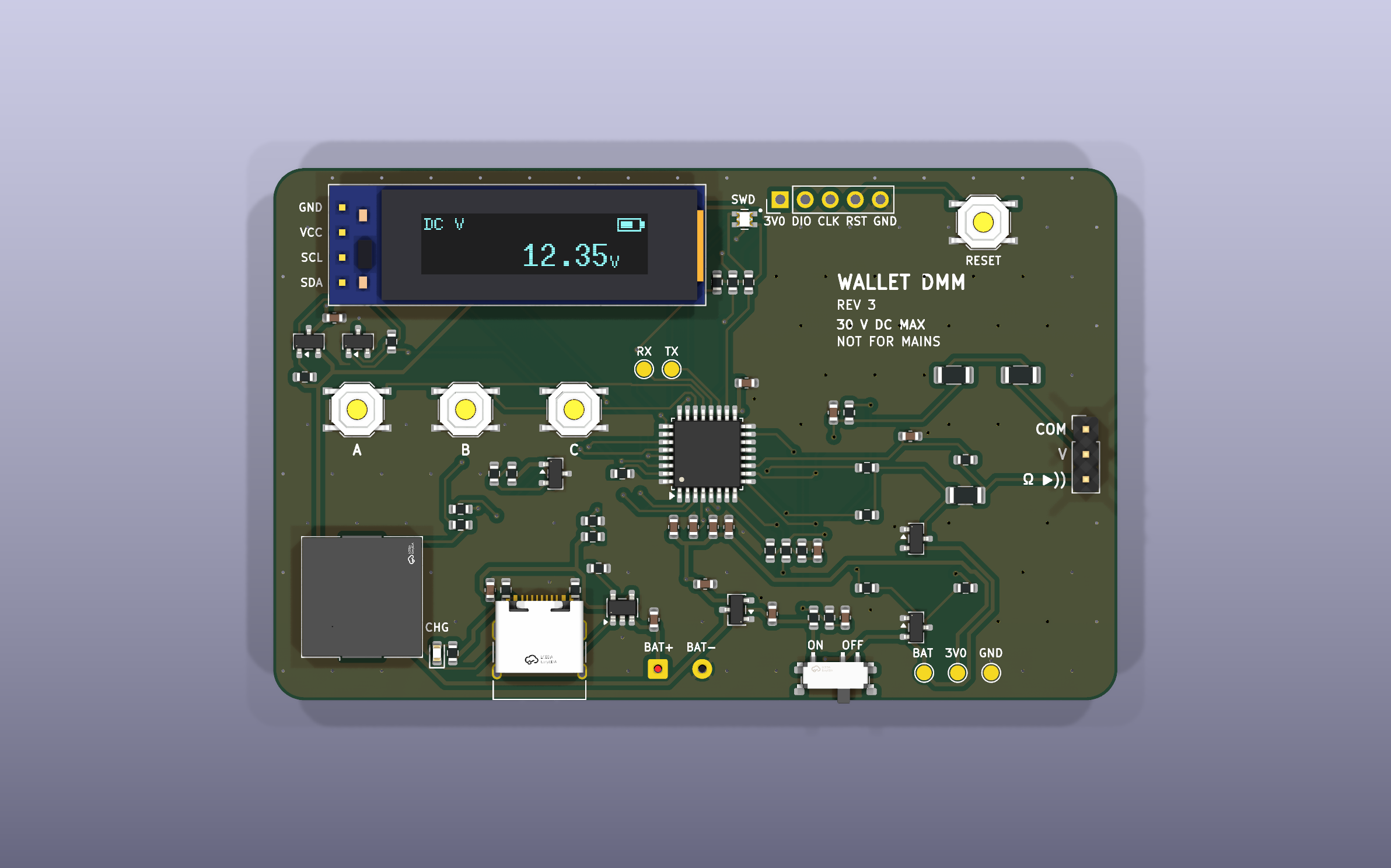
This is revision 3. Rev 1 (the October 2024 JLCPCB order) is commit a01ea68;
rev 2 is the v2 branch.
| Inputs | COM, V (10 MΩ) and Ω (resistance, continuity, diode) on a 2.54 mm header |
| Voltage | −30 V to +31 V; negative readings through a 1.55 V mid-rail bias |
| Resistance | 0–200 kΩ against a 0.1 % 10 kΩ reference, 150 kΩ–10 MΩ against 1 MΩ, autoranging |
| Continuity, diode | 0.3 mA test current, open-circuit 3.0 V |
| Overload | both inputs survive ±30 V DC; not for mains or anything above 30 V |
| Power | 3.7 V LiPo (protected cell), 100 mA USB-C charging, 3.0 V rail, about 5 µA off |
| Board | 85.6 × 54 mm (ID-1 card), 2 layers, 0.8 mm FR4 |
hardware/: KiCad 10 project (schematic, board, project rules, footprints
for the RGB LED and the OLED module, 3D models for every part)scripts/: generators for the schematic, board and 3D models, the
autorouter wrapper, the fab-file export and the rendersfab/: Gerbers, drill files, BOM and pick-and-place for JLCPCB, schematic
and assembly PDFsfirmware/: Rust firmware and its simulation (see
firmware/README.md)docs/: renders of the board and the simulation resultsEverything runs in the dev shell (nix develop, or direnv).
./scripts/build.sh # schematic -> ERC -> board -> DRC -> fab/The schematic and board are generated by scripts/gen_schematic.py and
scripts/gen_pcb.py; edit those rather than the KiCad files, or the next
build will overwrite the change. Tracks come from hardware/routes.json.
After moving parts or changing the netlist, route again with Freerouting:
kicad-cli sch export netlist --format kicadsexpr -o build/wallet_dmm.net hardware/wallet_dmm.kicad_sch
python3 scripts/autoroute.py build/wallet_dmm.net
The build stops on any ERC or DRC error and checks that the board matches the schematic.
The renders in docs/renders/ and a GLB of the populated board
(build/wallet_dmm.glb, for any glTF viewer) come from:
./scripts/render.shMost parts use KiCad's own 3D models; the switches, buzzer, USB-C socket and
RGB LED use the manufacturers' models (via EasyEDA). The OLED module and the
battery are drawn by scripts/gen_models.py, which lights the OLED's pixels
with the firmware's volts screen:
nix develop .#models -c uv run --with cadquery python scripts/gen_models.pyUpload fab/wallet_dmm-gerbers.zip: 2 layers, 0.8 mm, 1 oz, any colour,
HASL lead-free or ENIG. For assembly, choose top side and upload
fab/bom-jlcpcb.csv and fab/cpl-jlcpcb.csv. In the placement preview,
check the orientation of U1 (pin 1 dot), U2, U3, Q1, Q2, D2, D3, D1 (cathode)
and D4 (anode corner, the dot in the silkscreen) before confirming.
Solder these by hand afterwards:
A LiPo pouch cell with its own protection circuit, up to 30 × 40 × 4 mm, taped to the marked area on the back (no pins poke through there). Charging runs at 100 mA, so use 150 mAh or more; R3 sets the current (1000 V / R3).
scripts/gen_pcb.py.cal <volts> over the UART (TP2) to set the gain.The firmware is in firmware/: Rust and Embassy, with all the maths and the UI in a host-tested crate. Its README covers the buttons, calibration, flashing and the simulation. The pins:
| Pin | Use |
|---|---|
| PA0 ADC_IN0 | E_LO: the low-range drive node, through R18 |
| PA1 ADC_IN1 | VMID, the bias under the V divider |
| PA2 | VMID_EN: high while measuring volts |
| PA3 | OHM_HI: high-range drive (1 MΩ), analog otherwise |
| PA4 ADC_IN4 | V input divider |
| PA5 ADC_IN5 | Ω input, through R21 into C13 |
| PA6 | OHM_LO: low-range drive (10 kΩ), analog otherwise |
| PA7 | VBUS present (high on USB) |
| PB1 ADC_IN9 | switched battery ÷ 2 |
| PA8, PA15, PB3 | LED blue, red, green (low = on; PA15/PB3 are TIM2 CH1/CH2) |
| PB4, PB5 | piezo, TIM22 CH1/CH2 in antiphase, about 4 kHz |
| PB6, PB7 | I2C1 to the OLED (address 0x3C) |
| PC15 | OLED power: high = on |
| PA11, PA12, PC14 | buttons A, B, C to GND (enable pull-ups) |
| PA9, PA10 | USART1 TX/RX on TP1/TP2 |
firmware/simulate.sh runs the front end in ngspice, feeds it through a
model of the ADC into the firmware's own maths, and runs the release binary
in Renode on an emulated STM32L051. Across 200 simulated boards with 1 %
parts, calibrated volts are within ±4 mV up to ±5 V and ±33 mV at ±30 V,
and ohms within ±0.34 % from 1 kΩ to 100 kΩ. The details and plots are in
firmware/README.md and
docs/simulation/.

| Front | Back, with the battery |
|---|---|
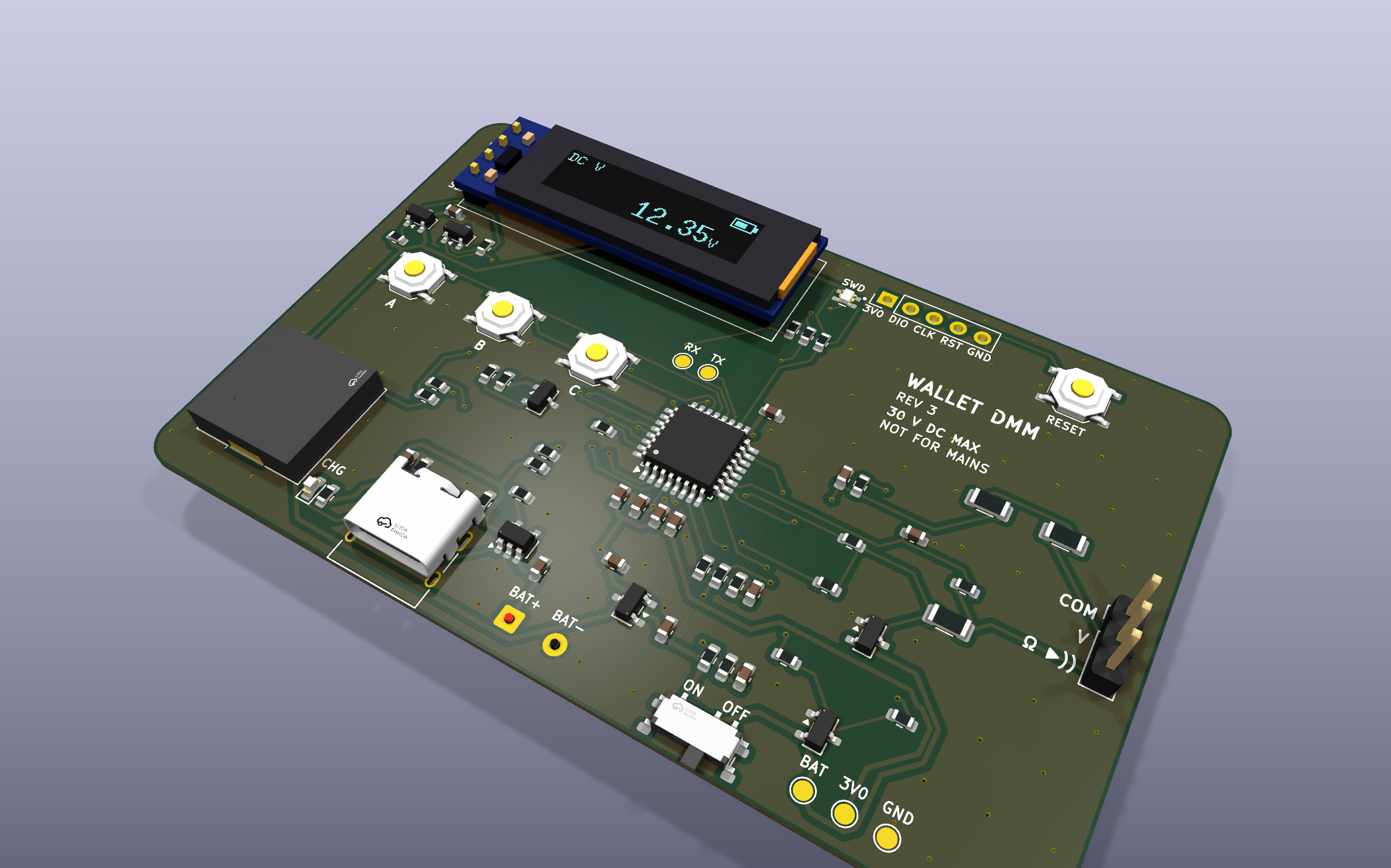 | 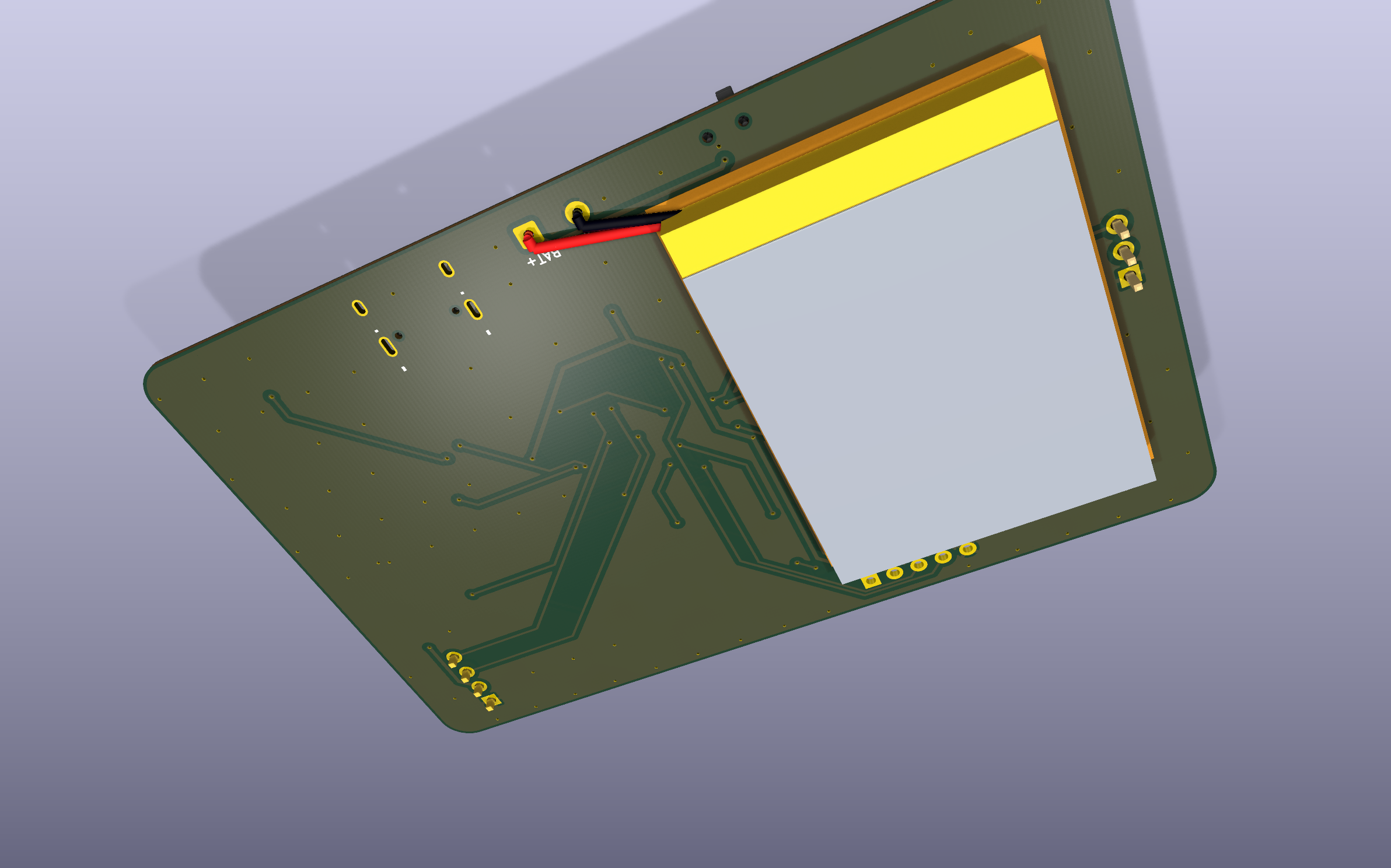 |
| Qty | Value | Footprint | References |
|---|---|---|---|
| 5 | 1k | Resistor_SMD:R_0603_1608Metric | R4, R15, R16, R19, R25 |
| 4 | 100nF | Capacitor_SMD:C_0603_1608Metric | C5, C6, C7, C10 |
| 4 | 10k | Resistor_SMD:R_0603_1608Metric | R3, R5, R9, R18 |
| 4 | 1M | Resistor_SMD:R_0603_1608Metric | R7, R8, R20, R30 |
| 4 | 1uF | Capacitor_SMD:C_0603_1608Metric | C3, C8, C12, C14 |
| 3 | 5.1k | Resistor_SMD:R_0603_1608Metric | R1, R2, R14 |
| 2 | 100k | Resistor_SMD:R_0603_1608Metric | R22, R23 |
| 2 | 220 | Resistor_SMD:R_0603_1608Metric | R27, R28 |
| 2 | 4.7M | Resistor_SMD:R_1206_3216Metric | R10, R11 |
| 2 | 4.7uF | Capacitor_SMD:C_0603_1608Metric | C1, C2 |
| 2 | BAV199 | Package_TO_SOT_SMD:SOT-23 | D2, D3 |
| 1 | 10k 0.1% | Resistor_SMD:R_1206_3216Metric | R17 |
| 1 | 10nF | Capacitor_SMD:C_0603_1608Metric | C9 |
| 1 | 10uF | Capacitor_SMD:C_0603_1608Metric | C4 |
| 1 | 15k | Resistor_SMD:R_0603_1608Metric | R6 |
| 1 | 22nF | Capacitor_SMD:C_0603_1608Metric | C13 |
| 1 | 2N7002 | Package_TO_SOT_SMD:SOT-23 | Q2 |
| 1 | 330 | Resistor_SMD:R_0603_1608Metric | R26 |
| 1 | 330k | Resistor_SMD:R_0603_1608Metric | R29 |
| 1 | 3V0 | TestPoint:TestPoint_Pad_D1.5mm | TP4 |
| 1 | 4.7k | Resistor_SMD:R_0603_1608Metric | R13 |
| 1 | 470k | Resistor_SMD:R_0603_1608Metric | R12 |
| 1 | 47k | Resistor_SMD:R_0603_1608Metric | R21 |
| 1 | 47nF | Capacitor_SMD:C_0603_1608Metric | C11 |
| 1 | 680 | Resistor_SMD:R_0603_1608Metric | R24 |
| 1 | AO3401A | Package_TO_SOT_SMD:SOT-23 | Q1 |
| 1 | BATT | TestPoint:TestPoint_Pad_D1.5mm | TP3 |
| 1 | BUTTON A | Button_Switch_SMD:SW_Push_1P1T_XKB_TS-1187A | SW1 |
| 1 | BUTTON B | Button_Switch_SMD:SW_Push_1P1T_XKB_TS-1187A | SW2 |
| 1 | BUTTON C | Button_Switch_SMD:SW_Push_1P1T_XKB_TS-1187A | SW3 |
| 1 | CHG red | LED_SMD:LED_0603_1608Metric | D1 |
| 1 | GND | TestPoint:TestPoint_Pad_D1.5mm | TP5 |
| 1 | LiPo 3.7 V | Connector_Wire:SolderWire-0.25sqmm_1x02_P4.5mm_D0.65mm_OD2mm | J5 |
| 1 | MCP73831T-2ACI/OT | Package_TO_SOT_SMD:SOT-23-5 | U2 |
| 1 | OLED 0.91in 128x32 I2C | wallet_dmm:OLED_0.91in_128x32_Module | J3 |
| 1 | PKLCS1212E4001 | Buzzer_Beeper:Buzzer_Murata_PKLCS1212E | BZ1 |
| 1 | POWER | Button_Switch_SMD:SW_SPDT_Shouhan_MSK12C02 | SW5 |
| 1 | PROBES | Connector_PinHeader_2.54mm:PinHeader_1x03_P2.54mm_Vertical | J2 |
| 1 | RESET | Button_Switch_SMD:SW_Push_1P1T_XKB_TS-1187A | SW4 |
| 1 | RGB | wallet_dmm:LED_RGB_1615_CA | D4 |
| 1 | STM32L051K8T6 | Package_QFP:LQFP-32_7x7mm_P0.8mm | U1 |
| 1 | SWD | Connector_PinHeader_2.54mm:PinHeader_1x05_P2.54mm_Vertical | J4 |
| 1 | TL431AIDBZR | Package_TO_SOT_SMD:SOT-23 | U4 |
| 1 | UART_RX | TestPoint:TestPoint_Pad_D1.5mm | TP2 |
| 1 | UART_TX | TestPoint:TestPoint_Pad_D1.5mm | TP1 |
| 1 | USB-C (charge only) | Connector_USB:USB_C_Receptacle_HRO_TYPE-C-31-M-12 | J1 |
| 1 | XC6206P302MR (3.0 V) | Package_TO_SOT_SMD:SOT-23-3 | U3 |
It measures 85.6 × 54 mm and has 2 copper layers, 0.8 mm thick.
70 parts, built around the STM32L051K8T6, MCP73831T-2ACI/OT-HXY, TL431AIDBZR and XC6206P302MR-G. The full list of its parts is on this page, with links to each part's symbol and footprint where PCBKit's library has them.
From the ArgonautGit/wallet_dmm repository on GitHub, at the commit this page was made from: the board is hardware/wallet_dmm.kicad_pcb and its schematic hardware/wallet_dmm.kicad_sch. PCBKit opens the board in the browser, with nothing to install.
Its repository states no licence, so its author keeps all rights: ask ArgonautGit before reusing the design.

leicht-io/BeoGram-4002-RIAA
Open-source RIAA phono preamp for the Bang & Olufsen BeoGram 4002/4004 turntable (KiCad)


Estylos/Light-Doorbell-HW
KiCad project for a custom, battery-powered doorbell with dual-color LED feedback and 4-layer circular PCB design. Optimized for low power and compact integration
