

2 layers158.5 × 119.3 mm

A 62-key split columnar ergonomic keyboard
Left is an open-source printed circuit board by andornaut, from the andornaut/splinter-keyboard repository on GitHub, published under the MIT licence. It is a 2-layer board of 160 × 118.5 mm with 67 parts on 52 nets, routed with 375 tracks and 67 vias.
It is built around the SMF5.0CA. Its parts include 31 diodes and 30 switches. It belongs with the keyboards and input boards of this library.


A 62-key split columnar ergonomic keyboard.
This repo holds the hardware design files; firmware lives in a separate repo. Design pipeline: Keyboard Layout Editor -> Ergogen -> KiCad -> fabrication -> Onshape -> OrcaSlicer -> QMK (see Developing).
Related notes: 3D printing, electronics, keyboards.
| Version | MCU | Changes from previous | Firmware | Photo |
|---|---|---|---|---|
| v4 | splitkb Liatris (RP2040) | Added USB VBUS detection and TRRS ESD protection | splinter | Pending |
| v3 | Adafruit KB2040 (RP2040) | Switched from AVR to RP2040 | splinter-v3.0 |  |
| v2 | SparkFun Pro Micro (ATmega32U4) | Symmetrical enclosures; added a key (62 keys) | splinter-2.0 |  |
| v1 | SparkFun Pro Micro (ATmega32U4) | Initial version: 61 keys, columnar layout, asymmetrical enclosures | splinter-1.0 |  |
Every version directory (v1/ .. v4/) follows the same shape, though not every version has every part:
| Path | Contents |
|---|---|
ergogen/config.yaml | Keyboard definition. The source of truth for everything downstream. |
ergogen/footprints/ | Symlink to the shared footprints below, so every version builds against one pinned set. Do not edit. |
keyboard-layout-editor/ | Layout prototypes. |
kicad/unrouted/ | Working boards. Ergogen generates into these; you route here. |
kicad/routed/ | Routed masters. The fab source. |
kicad/unrouted-backups/ | Timestamped copies of the unrouted/ boards, taken each time fresh ones overwrite them. Gitignored, and only the last few per board are kept. |
kicad/jlcpcb-parts.json | LCSC part numbers, kept outside the .kicad_pcb so they survive regeneration. v4 only, and what makes assembly files appear. |
onshape/ | Case design and its exported STEP. v4 adds the build sheet, the rationale, and a script that builds the same design as geometry and validates the export against it. |
orcaslicer/ | Slicer projects. v2 and v3 only. |
Shared across versions:
| Path | Contents |
|---|---|
ergogen/ | Footprints and helpers. |
scripts/ | Build steps. |
dist/ | Build output. Generated, not committed. |
A _ prefix on a PCB filename excludes it from every step.
| Tool | Needed for |
|---|---|
| KiCad 10 | Routing, and kicad-cli for gerber export and headless DRC |
| Node.js | Ergogen and the npm scripts |
| Python 3 | The build steps (stdlib only; pcbnew comes from KiCad) |
| OrcaSlicer | Slicing the printed case |
| FreeCAD | freecadcmd, for validating the case export |
| Freerouting | Optional, for autorouting |
| KiKit | Optional, for panelization; needs the git-master build |
# Include submodules when cloning
git clone --recursive git@github.com:andornaut/splinter-keyboard.git
cd splinter-keyboard

# Install the Node version from .nvmrc, then the deps (including Ergogen)
nvm install
npm install

# Install KiCad 10 (provides kicad-cli, used for fab file generation)
sudo add-apt-repository ppa:kicad/kicad-10.0-releases
sudo apt install kicad

# Fallback only if you cloned without --recursive
git submodule update --init --recursive
OrcaSlicer, FreeCAD, KiCad, Freerouting and KiKit also install from these Ansible tasks (tags orcaslicer, freecad and kicad; Freerouting and KiKit come with kicad).
Updating footprint submodules. npm run ergogen uses ceoloide and infused-kim at their pinned revision and never advances them, so builds stay reproducible. To re-pin:
git submodule update --remote ergogen/footprints/ceoloide ergogen/footprints/infused-kim
git add ergogen/footprints/ceoloide ergogen/footprints/infused-kim
git commit -m "Bump footprint submodules"Run everything through npm run from the repo root: the scripts read the active version from config.VERSION in package.json.
| Command | Does |
|---|---|
pipeline | The full build, every gate in order. The normal entry point. Add -- -v for the full log. |
ergogen | Generate outlines and PCBs into dist/${VERSION}/ergogen/ |
watch / watch:sync-unrouted | Re-run ergogen on every config.yaml change, the second also copying into unrouted/ |
copy:dist-to-unrouted | dist/ -> unrouted/ (backs the old boards up to unrouted-backups/ first) |
copy:traces-to-unrouted | Traces and teardrops from routed/ back into unrouted/ |
copy:unrouted-to-routed | unrouted/ -> routed/ (see Saving to routed/) |
fab | Gerbers, drill, and assembly BOM/CPL via kicad-cli |
panelize | Combine both halves into one JLCPCB panel (optional) |
route | Autoroute unrouted/ via Freerouting (optional) |
validate:provenance / validate:symmetry / validate:firmware / validate:fab | The four gates (see Validation) |
clean | Remove dist/ |
lint / format | Prettier and ESLint, checking or fixing. lint is a CI gate |
Set config.VERSION in package.json to v1, v2, v3, or v4, by editing the file or with npm pkg set config.VERSION=v4.
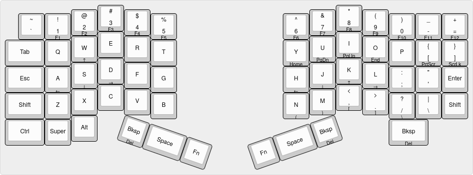
Prototype a layout, export it to keyboard-layout-editor.json so you can re-import and iterate, then use it as the basis for the Ergogen design. To load it into the Raw data tab, paste it without its outer [ and ]: the tab takes the layout's rows directly, while the downloaded JSON wraps them in an array.
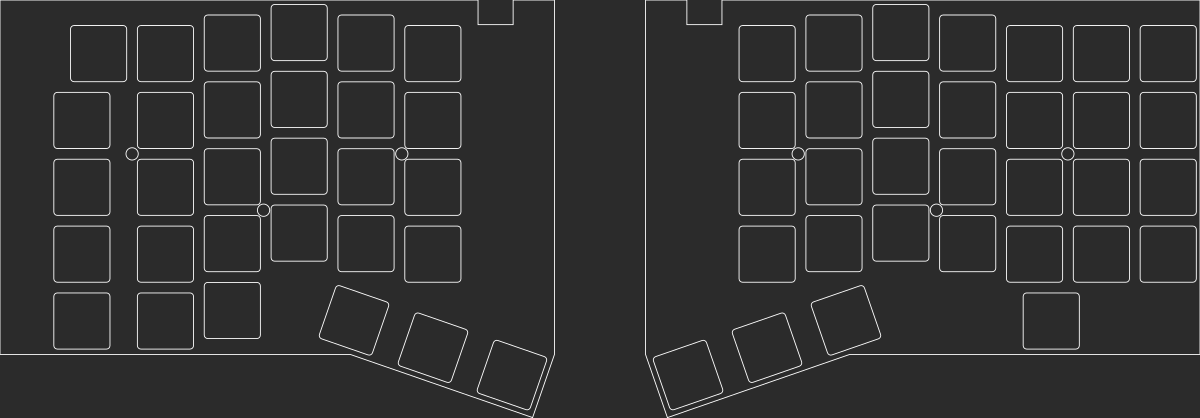
docker compose up starts the Ergogen GUI (it builds on first run); open http://ergogen.internal (needs docker_etc_hosts for the /etc/hosts entry).ergogen/config.yaml.npm run ergogen, then npm run copy:dist-to-unrouted. Or just npm run watch:sync-unrouted.config.yaml (the source of truth), build with npm run ergogen.Dockerfile bakes this repo's custom footprints into the GUI image. An unregistered what: shows up as unknown; after adding one, docker compose build --no-cache.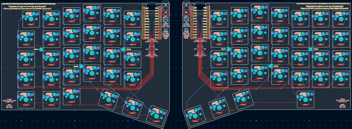
Open a board from kicad/unrouted/ and route it. Before saving:
npm run fab re-runs it headlessly, but fixing it here beats reading the JSON.After regenerating with Ergogen, npm run copy:traces-to-unrouted brings the traces and teardrops from routed/ back into unrouted/ (then File > Revert in KiCad).
npm run copy:unrouted-to-routed writes the masters' .kicad_pro and .kicad_dru first, since the stages that move copper measure against the clearances those hold. Then, one master at a time, it copies the working board onto its master in kicad/routed/ and runs:
| Stage | What it does |
|---|---|
| GND pour | Floods a ground plane on whichever side costs less (scored per board, F.Cu vs B.Cu) |
| Cleanup | Strips copper no route uses: dangling tracks and the vias they strand, tracks buried in pads, redundant vias, split segments |
| Pattern snap | Pulls strays onto the repeated shape they belong to, within a per-endpoint cap |
| Sliver tidy | Collapses any segment left shorter than it is wide, within a per-endpoint cap |
One master at a time, copy included, because any stage can stop the build: a master this run has not reached yet is still the routed board it was, rather than an un-poured working copy that nothing downstream would catch.
The last three stages feed each other: a collapsed sliver can leave a run the next snap recognises, and a snap leaves fragments for the next cleanup to merge and can leave a sliver of its own. So they repeat until a pass changes nothing, and a board still changing on the last allowed pass stops the build instead of shipping a master its own tooling has not finished with.
The working boards keep the stripped copper, mainly the footprints' unused include_traces_vias stubs, since a later reroute may pick it up.
Pattern snap and sliver tidy move copper rather than only removing it, so both are capped and neither guesses: pattern snap reports a stray it may not move and leaves it, while sliver tidy stops the build:
KiCad has no built-in autorouter. npm run route routes the unrouted/ boards in place via Freerouting, leaving routed/ untouched; expect to hand-clean the result, then File > Revert. Raising via cost trades vias for unrouted nets, so it cannot beat hand-routing on via count.
| Env var | Default | Values |
|---|---|---|
FREEROUTING_PASSES | 100 | |
FREEROUTING_STRATEGY | greedy | greedy, global, hybrid |
FREEROUTING_SELECTION | prioritized | prioritized, random, sequential |
FREEROUTING_VIA_COST | 50 | higher = fewer vias |
FREEROUTING_UNDESIRED_DIR_COST | unset | cost of routing against a layer's preferred direction |
FREEROUTING_LOG_LEVEL | WARN | ERROR, WARN, INFO, DEBUG, TRACE |
npm run fab exports from routed/ into dist/${VERSION}/kicad/jlcpcb/<name>/:
| Output | Contents |
|---|---|
<name>-gerber.zip | Gerbers and drill: the bare PCB |
<name>-BOM.csv, <name>-CPL.csv | Assembly files, written only when jlcpcb-parts.json is present |
<name>-drc.json | Headless DRC report, written per board before that board's export. Any error-level violation or unrouted net stops the run there, so a failing board never overwrites its own last-good gerbers. |
A provenance check gates the whole run before any board is touched, so a master that drifted from config.yaml produces nothing at all.
Which parts JLCPCB places and which you hand-solder is version-specific; see the v4 notes.
Ordering from JLCPCB: upload each <name>-gerber.zip, plus the matching BOM and CPL for assembly. Check placement in the DFM viewer; fix a mis-oriented part via its rotation in jlcpcb-parts.json and re-run.
npm run panelize combines left and right into one panel so JLCPCB's per-order assembly setup and stencil fees are paid once instead of twice. The panel is not orderable yet: its frame is not tabbed to the boards, and its fiducials sit on its tooling holes at the rail's inner edge. Order the halves separately until scripts/panelize.py is fixed. Outputs to dist/${VERSION}/kicad/jlcpcb/panel/; the per-half fab remains the strict DRC gate. Requires KiKit (git-master build for KiCad 10); point it at an interpreter with KIKIT_PYTHON.
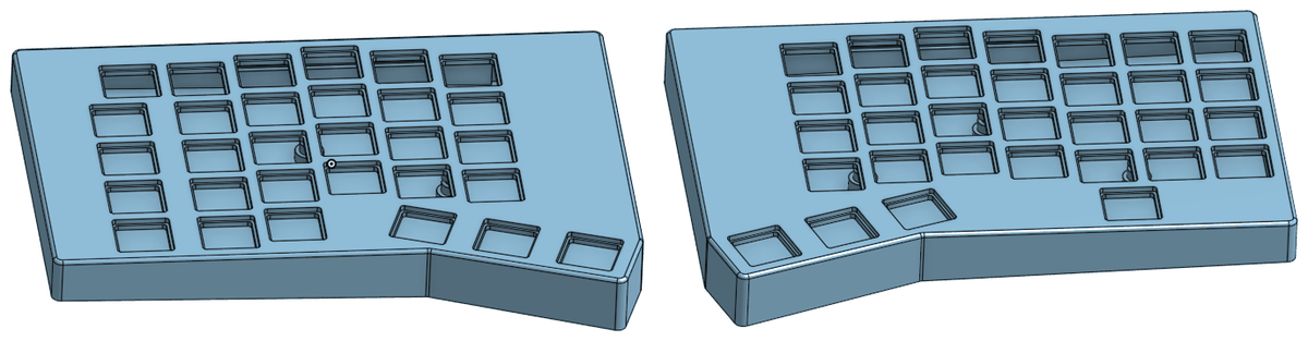
dist/${VERSION}/ergogen/outlines/full_unfilleted.dxf. That is the nominal hull rather than the fabricated edge: the fillet only removes material, so a pocket cut to the hull can never come out undersized.onshape/BUILD.md, which carries every dimension and the feature-by-feature recipe, then export it to dist/${VERSION}/onshape/.FC_HALF=left FC_COMPARE=dist/${VERSION}/onshape/<export>.step freecadcmd v4/onshape/gen-case.py and again with FC_HALF=right, and decide every difference it reports: move the model to the reference, record it in v4/onshape/differences.json as intentional, or fix it as an error. See Validating your model.v4/onshape/Splinter keyboard v4 - Filament.step. Validate the aluminium configuration's export the same way with FC_VARIANT=aluminium added, then copy it over Splinter keyboard v4 - Aluminium.step.FC_VARIANT=aluminium FC_COMPARE=<shell>.step,<plate>.step, and copy them over v4/onshape/Splinter keyboard v4 - Aluminium - {Left,Right} {shell,plate}.step.Splinter keyboard v4 - Filament.step.Upload the model's aluminium configuration (tapped holes, see Aluminium variant) to JLCCNC as four files, one part each, since JLCCNC quotes per file: Splinter keyboard v4 - Aluminium - Left shell.step, Splinter keyboard v4 - Aluminium - Left plate.step, Splinter keyboard v4 - Aluminium - Right shell.step and Splinter keyboard v4 - Aluminium - Right plate.step. Attach each part's drawing to that part, and quote each part once:
| Setting | Value |
|---|---|
| Material | 6061 aluminium (JLCCNC's standard alloy) |
| Surface finish | Bead blasting + anodizing, dark grey. Order all four parts together so they anodize in one batch and match |
| Tolerance | Select +-0.1 on all four parts, and mark the mating dimensions +-0.1 on each part's drawing: JLCCNC applies a selected tolerance only to dimensions annotated on the 2D drawing, and everything else defaults to ISO 2768 medium (+-0.5 above 120mm, more than the plate's 0.40 total clearance in its cavity). The drawings dimension between straight edges: the shell cavity 161.00 wide and 102.25 tall at its outer side, the plate 160.60 and 101.85. Holes are placed from mating edges, listed outer / centre / inner hole. The shells: from the cavity's outer side (38.13, 77.18, 114.33), and from the cavity edge opposite the thumb (63.65, 37.83, 59.95). The plates: from the plate's outer side (37.93, 76.98, 114.13) and its thumb-side edge (38.40, 64.23, 42.10) |
| Threaded holes | Threads YES on each shell: 3 x M2.5x0.45. Threads NO on the plates. Attach every part's PDF by hand: the PDFs are not named like the STEPs. The heat-set inserts are for the printed case only |
| Order remarks | Shells: "Threads: 3 x M2.5x0.45 blind, 2.05 drill 4.00 deep, full thread to 2.65 required (screw reaches 2.53). If you can't hold 2.65, contact me before machining." Plates: "Fits into the matching shell's cavity with 0.20/side clearance; its three 2.90 holes must line up with the shell's tapped holes." |
| Edges | JLCCNC breaks external edges by about 0.2 by default. The drawings' title block says only "REMOVE BURRS", so that default applies to the switch recess rims too, which the model leaves square |
A STEP file cannot carry threads, so model each hole at the ~2.05mm tap-drill diameter and upload a PDF with an M2.5x0.45 callout, 4.00 drill and full thread to 2.65: the drill leaves 1.35 of run-out below the full thread, more than half the diameter, so a standard tap reaches it. Every hole shares the thread spec and the depth, so one callout covers all three; take both from the build sheet. Splinter v4 left shell.pdf and Splinter v4 right shell.pdf carry the thread callouts and the +-0.1 annotations above; Splinter v4 left plate.pdf and Splinter v4 right plate.pdf carry the annotations only. To redraw one, make an Onshape Drawing of the Aluminium configuration and use its Hole callout tool on a tapped hole's edge; it reads the spec from the Hole feature.
Install the custom QMK firmware.
npm run pipeline re-syncs already-routed boards after a config change:
| # | Step | Does |
|---|---|---|
| 1 | ergogen | Rebuild the boards from config.yaml |
| 2 | copy:dist-to-unrouted | Fresh boards into unrouted/, old ones backed up |
| 3 | copy:traces-to-unrouted | Replay the masters' routing onto them |
| 4 | copy:unrouted-to-routed | Save back to routed/ (details) |
| 5 | validate:provenance | Stamps match config.yaml |
| 6 | validate:symmetry | The halves are exact mirror images |
| 7 | validate:firmware | Boards match the QMK matrix |
| 8 | fab | Export gerbers and assembly files |
| 9 | validate:fab | Audit those outputs |
Every step is a hard gate. panelize runs last and is the only optional one, skipped with a note when KiKit is absent.
A step reports what it changed and what wants reading; lines that only confirm nothing needed doing are held back, since each step's closing OK: line already carries the count they would have added up to. npm run pipeline -- -v shows them all, plus Ergogen's own narration and the artifact listing file by file.
It requires existing routed masters and does not route for you: step 3 replays their traces onto the fresh boards and aborts if a master carries no human routing. For a first route, or when geometry moves enough that the old traces no longer fit, route by hand in KiCad (Step 4).
| Gate | Checks |
|---|---|
validate:provenance | Every board's stamp still matches config.yaml, and the boards in a stage were all built in the same run, so neither a stale master nor a half restored on its own can reach fab |
validate:symmetry | The two halves are exact mirror images: outline, parts, pads, rule areas and silk, compared in each board's own frame so the per-board recentering is not read as asymmetry |
validate:firmware | Both halves wire the MCU header identically, and the matrix they imply equals the QMK keyboard.json |
validate:fab | The exported artifacts: a board-spanning GND plane on both master and gerbers, a complete gerber set, a non-empty BOM and CPL with every assembled footprint appearing in the CPL exactly once, outputs no older than their sources, comparable teardrop counts across the halves |
validate:fab also warns, without failing, when a master was built from an uncommitted tree: the board is fine, but its recorded commit means nothing, so the warning is expected during ordinary in-progress work.
validate:symmetry holds the halves to being exact mirrors of each other. The licensed exception is the keys of the outer pinky columns, which differ by design (the left pinky is 1.5u; the right is 1u plus an extra inner column). Drift here is otherwise invisible: both halves still route, pass DRC, fab and assemble, and it surfaces only as a case that fits one half and rocks on the other, or a clearance that is comfortable on one half and marginal on the other. Both halves are generated from one set of mirrored anchors in config.yaml, so a failure is a config change to undo rather than a board to edit.
Four kinds of part are placed in the same orientation on both halves rather than mirrored, because the parts themselves cannot be: an MX switch and its Kailh socket have an asymmetric pin pattern, the matrix diode wires straight to a switch pin and follows it, the MCU is a module that plugs in one way up, and the TRRS jack mounts on the back of both halves with the same pin pattern. Their pads therefore land at mirrored positions carrying the opposite pin at each. Key placements still mirror exactly, and so does every clearance measured from key geometry; only pad-to-edge distances within a key differ between the halves. Hand routing is not compared at all.
validate:firmware reads the keyboard.json at config.FIRMWARE in package.json, which ships as a path to a sibling qmk_firmware checkout so the check covers what you are about to flash rather than what is pushed. Without that checkout the step fails and no gerbers are produced; pass --firmware <url|path> or set $SPLINTER_FIRMWARE_JSON instead.
The copy steps and manual routing let routed/ drift from config.yaml, so you could fab a stale board. npm run ergogen stamps each board with a hash of config.yaml; fab refuses a drifted or unstamped master, and validate:provenance checks without fabbing. Clear a mismatch by re-running the pipeline, re-routing if needed.
Restoring or rebuilding one half on its own is invisible to the hash, since identical config bytes hash the same across builds, so validate:provenance also requires every board in a stage to carry the same stamp. The two stages are compared separately: unrouted/ is expected to be newer than routed/ between an ergogen run and the save back to the masters.
A panel inherits its masters' stamp rather than getting one of its own, so its commit= names the commit the panelled copper came from. Masters whose stamps disagree stop panelize, since a panel merged from two generations of board has no single provenance to report.
Only config.yaml is hashed, so a footprint .js or Ergogen-version change can move geometry without tripping the check, while a comment-only config edit trips a false "stale".
A stamp names the commit the build's inputs came from, never the commit that contains the stamped board: the stamp is written into the board, so it can only name its own parent. To get the boards a stamp describes, check that commit out and rebuild.
git checkout <the commit= from the stamp>
npm run pipeline
Taking kicad/routed/*.kicad_pcb straight from that commit instead gives you the previous build's masters. Rebuilding reproduces copper, drill, mask, paste, outline and the assembly files identically; only the built= timestamp drawn on the silk and a few microns of teardrop fill tessellation differ.
| Qty | Value | Footprint | References |
|---|---|---|---|
| 30 | ceoloide:switch_mx | S1, S2, S10, S11, S12, S13, S14, S15, S16, S17, S18, S19, S20, S21, S22, S23 +14 | |
| 30 | splinter:diode_sod123 | D1, D2, D10, D11, D12, D13, D14, D15, D16, D17, D18, D19, D20, D21, D22, D23 +14 | |
| 3 | ceoloide:mounting_hole_npth | MH1, MH2, MH3 | |
| 1 | splinter:mcu_liatris | MCU1 | |
| 1 | splinter:trrs_hc_pj320a | TRRS1 | |
| 1 | E73:SW_TACT_ALPS_SKQGABE010 | B1 | |
| 1 | SMF5.0CA | splinter:D_SOD-123FL | D31 |
It measures 160 × 118.5 mm and has 2 copper layers, 1.6 mm thick.
67 parts, built around the SMF5.0CA. The full list of its parts is on this page, with links to each part's symbol and footprint where PCBKit's library has them.
From the andornaut/splinter-keyboard repository on GitHub, at the commit this page was made from: the board is v4/kicad/unrouted/left.kicad_pcb. PCBKit opens the board in the browser, with nothing to install.
Its repository publishes it under the MIT licence: you may reuse it on that licence's terms (keep the author's notice, and for a copyleft licence share your changes alike).


atomicra1n/wifi-geiger-counter
A DIY Geiger counter PCB which can detect ionizing radiation and log readings over Wi-Fi. Built with an ESP32, and a HV multiplier circuit that steps up 3.7V to 400V for the GM tube.

bartkepl/RDE_board
Resistance DEcade with SCPI, UART, USB, RS485 and ETHERNET in 3U eurocard format


bartkepl/UCB_board
Control board for testing concepts with SCPI, UART, USB, RS485 and ETHERNET in pseudo 3U eurocard format

danhmanu/PLC-STM32F407VET6
Mạch nguyên lý KiCad 10 cho bộ PLC: điều khiển qua LAN bằng Modbus TCP (module W5500 Lite), nạp code qua USB‑C (CH340C), 16 ngõ ra transistor cách ly quang, 10 ngõ vào analog 4–20mA.