Skip to the content
PCBKitNew board
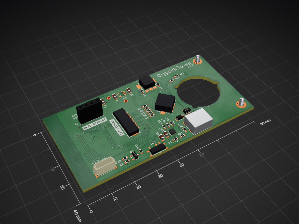
2 layers80 × 40 mmCryptick token pcb, the printed circuit board in 3D

Hardware schematics, 2-layer PCB layout, and manufacturing files for Cryptick Token — the 100% open-source biometric hardware security key and cryptographic hardware enclave.

Size
80 × 40 mm
Copper layers
2
Thickness
1.6 mm
Parts
56
Nets
73
Pads
303
Tracks, vias
640, 93
Pours
3
Routed
Yes
KiCad
KiCad 10.0 (file 20260206)
Created
21 Jul 2026
Updated
19 Oct 2026

Overview

Cryptick token pcb is an open-source printed circuit board by alphaseneca, from the alphaseneca/cryptick-token-pcb repository on GitHub, published under the MIT licence. It is a 2-layer board of 80 × 40 mm with 56 parts on 73 nets, routed with 640 tracks and 93 vias.

It is built around the ESP32-S3-WROOM-1-N8, BQ25185DLHR and DS3231MZ+TRL, with the ME6217C33M5G, USBLC6-2SC6 and AP3404 among its other parts. Its parts include 21 resistors, 10 capacitors, 6 connectors, 5 ICs and 3 switches. It belongs with the ESP32 boards of this library.

Main components

12

README

README.md

Cryptick Token Hardware PCB

Manufacturing Release License: MIT KiCad

Hardware schematics, 2-layer PCB layout, and manufacturing files for Cryptick Token — the 100% open-source biometric hardware security key and cryptographic hardware enclave.


Hardware Highlights

  • Main Processing Unit: Espressif ESP32-S3-WROOM-1 (N16R8) Dual-Core Xtensa LX7 @ 240 MHz with hardware cryptography accelerators (AES-256, SHA-256, RSA-3072, ECC point multiplication, TRNG) and 16 MB encrypted SPI Flash.
  • Biometric Security Enclave: R558S optical/capacitive fingerprint sensor connector (J4, 6-pin JST SH) wired for UART (TX GPIO 17, RX GPIO 18) plus a hardware wake-on-touch interrupt on GPIO 16. (Sensor-internal specs such as DPI and template capacity come from the module's own datasheet, not this schematic, and are not re-verified here.)
  • Physical WYSIWYS Display: Driven primarily through a 20-pin FPC connector (FPC1) — SPI (CS0 GPIO 10, SCK GPIO 12, SDO GPIO 11), RS/RESET on GPIO 47/48, and a GPIO 42-switched NMOS LED backlight (Q1) — with a touch-controller interrupt/reset pair on GPIO 1/2. A secondary 4-pin I2C header (J3, labeled "OLED Display" in the schematic) taps the same I2C bus (SDA GPIO 8, SCL GPIO 9). See docs/ARCHITECTURE.md for the full netlist-verified wiring — the specific panel controller IC and pixel resolution are not encoded anywhere in the KiCad source, so they are not asserted here.
  • Real-Time Clock: Maxim DS3231M I2C RTC (±5ppm, U1) on the shared I2C bus, with its own coin-cell backup supply (BT1) so it keeps time through power loss — the time source behind this device's TOTP codes.
  • Physical Navigation: 5-Way Tactile Navigation Switch (SW1, net labels /UP→GPIO6, /DOWN→GPIO5, /LEFT→GPIO7, /RIGHT→GPIO4, /CENTER→GPIO15 per the schematic's own net names) for tactile PIN entry, menu navigation, and physical user presence (UP) confirmation, plus an ALPS EC05E1220401 quadrature rotary encoder (SW2, channel A/CW on GPIO 40, channel B/CCW on GPIO 41) for scroll navigation. The encoder's integrated pushbutton is wired straight to GND on this revision, not to a GPIO — there is no separate "encoder click" signal.

    Known conflict, not yet resolved — do not treat either source as settled: the firmware's include/board_config.h assigns UP_BUTTON_PIN=7, LEFT_BUTTON_PIN=6 (GPIO4/5 for RIGHT/DOWN match), the opposite of this schematic's /UP//LEFT net labels, with a comment dated 2026-08-08 citing an actual flashed-hardware bring-up log as the source ("pairs were swapped vs first silk guess — UP↔LEFT... corrected here"). That firmware pin map predates this schematic re-read and was reportedly verified against a real, physically assembled board — a schematic net name only records what the designer called a pad, not which way the switch's internal actuator physically moves it, so a live bring-up test is the stronger of the two sources in general. But this schematic's current net names weren't re-verified against actual silkscreen/part orientation either. Do not change board_config.h to match the net names above without confirming on real hardware first — if the firmware mapping is the one that's actually correct, "fixing" it to match this schematic would swap UP/LEFT and DOWN/RIGHT on a real device.

  • Wireless & Wired Interfaces:
    • Bluetooth Low Energy (BLE 5.0) via onboard 2.4 GHz PCB antenna.
    • Native USB Type-C Receptacle (USB 2.0 Full-Speed OTG) with bidirectional TVS diode ESD protection (USBLC6-2SC6).
  • Power Management:
    • TI BQ25185DLHR LiPo/Li-Ion linear battery charge management with dual status monitoring (STAT1 GPIO 38, STAT2 GPIO 39).
    • High-efficiency 3.3V LDO regulator with low quiescent current for ultra-deep sleep.
    • Single fixed (non-addressable) power-present LED (D1, 0603). GPIO48/PIN_NEOPIXEL is generic ESP32-S3 Arduino-variant boilerplate inherited from a reference dev-board file — there is no WS2812B or any addressable RGB LED on this board.

PCB Specifications

ParameterSpecification
Dimensions80.0 mm × 40.0 mm × 1.6 mm
Layer Count2 Layers (F.Cu Signal / B.Cu Signal, no internal plane layers)
Copper Weight1 oz (both layers)
Min Trace / Space0.127 mm / 0.127 mm (5/5 mil)
Surface FinishENIG (Electroless Nickel Immersion Gold) - RoHS compliant
Solder MaskMatte Black with Gold Traces
SilkscreenHigh-definition White
Design RulesJLCPCB 2-Layer Standard (exact process code not re-verified here — confirm against JLCPCB's current capability page before ordering; JLC04161H-7628 was wrong, that's a 4-layer code)

Schematic & Manufacturing Files

  • Schematic source: cryptick-token-pcb.kicad_sch
  • Board layout: cryptick-token-pcb.kicad_pcb
  • KiCad project: cryptick-token-pcb.kicad_pro
  • Hardware architecture overview & block diagram: docs/ARCHITECTURE.md
  • Automated releases produce:
    • Gerber RS-274X drill and layer files (gerbers.zip)
    • Bill of Materials (BOM) in JLCPCB SMT format (bom.csv)
    • Pick and Place Component Centroid coordinates (pos.csv)

Automated Tag Release

Pushing any semantic version tag (e.g. v0.1.0) triggers .github/workflows/release.yml, executing KiForge in CI to automatically generate and attach production fabrication assets to GitHub Releases.


License

Hardware schematics and PCB designs are licensed under the MIT License / CERN Open Hardware Licence.
Parts

56
QtyValueFootprintReferences
1110KResistor_SMD:R_0603_1608MetricR1, R2, R3, R4, R5, R6, R7, R8, R10, R20, R21
41KResistor_SMD:R_0603_1608MetricR14, R15, R17, R19
310uCapacitor_SMD:C_0805_2012MetricC3, C7, C8
31uCapacitor_SMD:C_0805_2012MetricC2, C9, C10
222RResistor_SMD:R_0603_1608MetricR16, R18
222uCapacitor_SMD:C_0805_2012MetricC1, C4
25K1Resistor_SMD:R_0603_1608MetricR12, R13
2MountingHole_PadMountingHole:MountingHole_2.2mm_M2_Pad_ViaH1, H2
1100RResistor_SMD:R_0603_1608MetricR9
1100nCapacitor_SMD:C_0805_2012MetricC5
110RResistor_SMD:R_0603_1608MetricR11
133pCapacitor_SMD:C_0805_2012MetricC6
15VLED_SMD:LED_0603_1608MetricD1
1AP3404Package_TO_SOT_SMD:SOT-23-3Q1
1BQ25185DLHReasyeda2kicad:WSON-10_L2.2-W2.0-P0.40-BL-EP_TI_DLH0010AU4
1BS-12-A1AJ002-Feasyeda2kicad:BAT-TH_BS-12-A1AJ002-FBT1
1DS3231MZPackage_SO:SOIC-8_3.9x4.9mm_P1.27mmU1
1EC05E1220401easyeda2kicad:SW-SMD_EC05E1220401SW2
1ESP32-S3-WROOM-1RF_Module:ESP32-S3-WROOM-1U2
1FPC-05F-20PH20easyeda2kicad:FPC-SMD_20P-P0.50_XUNPU_FPC-05F-20PH20FPC1
1Fingerprint_SensorConnector_JST:JST_SH_BM06B-SRSS-TB_1x06-1MP_P1.00mm_VerticalJ4
1G***kibuzzard-6A3445EBkibuzzard-6A3445EB
1G***kibuzzard-6A344DA8kibuzzard-6A344DA8
1G***kibuzzard-6A344627kibuzzard-6A344627
1JST-6 PIN-JST-SHConnector_JST:JST_SH_BM06B-SRSS-TB_1x06-1MP_P1.00mm_VerticalJ5
1K1-5202UA-01easyeda2kicad:SW-SMD_K1-5202UA-01SW1
1LOGOassets:ucaseG***
1ME6217C33M5Geasyeda2kicad:SOT-23-5_L3.0-W1.7-P0.95-LS2.8-BRU3
1MSK12C02-HBeasyeda2kicad:SW-TH_MSK12C02-HB-1SW3
1OLED DISPLAYConnector_PinHeader_2.54mm:PinHeader_1x04_P2.54mm_VerticalJ3
1PTVS5V0S1URDiode_SMD:D_SOD-123D2
1SM02B-SRSS-TBeasyeda2kicad:CONN-SMD_2P-P1.00_SM02B-SRSS-TB-LF-SNCN2
1USBLC6-2SC6Package_TO_SOT_SMD:SOT-23-6U5
1USB_C_Receptacle_USB2.0_16PConnector_USB:USB_C_Receptacle_G-Switch_GT-USB-7010ASVJ1
1YXT-BB10-24S-02easyeda2kicad:CONN-SMD_YXT-BB10-24S-02CN1

Questions

How big is the Cryptick token pcb PCB?

It measures 80 × 40 mm and has 2 copper layers, 1.6 mm thick.

What parts does the Cryptick token pcb use?

56 parts, built around the ESP32-S3-WROOM-1-N8, BQ25185DLHR, DS3231MZ+TRL and ME6217C33M5G. The full list of its parts is on this page, with links to each part's symbol and footprint where PCBKit's library has them.

Where can I download the Cryptick token pcb KiCad files?

From the alphaseneca/cryptick-token-pcb repository on GitHub, at the commit this page was made from: the board is cryptick-token-pcb.kicad_pcb and its schematic cryptick-token-pcb.kicad_sch. PCBKit opens the board in the browser, with nothing to install.

Can I use the Cryptick token pcb design in my own project?

Its repository publishes it under the MIT licence: you may reuse it on that licence's terms (keep the author's notice, and for a copyleft licence share your changes alike).

Similar boards

  • 2 layers128.7 × 60.3 mmMOBILE, the printed circuit board in 3D

    MOBILE

    sumit123hub/Mobile-PCB-Files-

    I always dreamed of building my own mobile system. This repo documents my journey designing a custom ESP32 PCB featuring a GSM module, display interface, and complete Battery Management System (BMS).

    92 parts
  • 2 layers97 × 97 mmPCBA ZONA LED, the printed circuit board in 3D

    PCBA ZONA LED

    intechstudio/grid-hardware

    259 parts59GPL-3.0
  • 2 layers51.1 × 50 mmWheelchair ui, the printed circuit board in 3D

    Wheelchair ui

    coencoelectronics/WheelChairUI_PCB

    53 parts
  • 4 layers160 × 115 mmSjc, the printed circuit board in 3D

    Sjc

    tgiacomellibr/sjc

    Single Joint Control Board

    346 partsMIT
  • 4 layers15 × 80 mmWand, the printed circuit board in 3D

    Wand

    JMET04/aicad-agent

    Deterministic CAD/EDA agent plugin for 2D drawings, AutoCAD, SolidWorks, KiCad, review gates and auditable delivery.

    46 parts1MIT
  • 2 layers40 × 40 mmToytalker mini v0.1, the printed circuit board in 3D

    Toytalker mini v0.1

    tomonoriyamazaki/toytalker

    AI voice companion toy for kids

    38 parts
  • 4 layers28.7 × 27 mmNeurband c, the printed circuit board in 3D

    Neurband c

    jlcjak/neurband

    Open, minimal sEMG wristband like the Meta Neural Band: 8-ch ADS1298 + nRF52832 BLE, dry gold electrodes on a flex, 3D-printed band. KiCad, FreeCAD, Zephyr, Python, simulations.

    70 parts46