2 layers148 × 84.5 mm
Panel daisy
ohmtech-rdi/eurorack-blocks
Software to Hardware Prototyping for Eurorack using C++, Max/Gen~ or Faust
259 parts410

 aliihsan1913/Analog-HH-Neuron
Instead of utilizing microprocessors or algorithmic software to approximate the differential equations, this circuit solves the time and voltage-dependent variables ($V, m, h, n$) in real-time using the inherent…
Neuromorphic Soma Node is an open-source printed circuit board by aliihsan1913, from the aliihsan1913/Analog-HH-Neuron repository on GitHub, published under the MIT licence. It is a 2-layer board of 60.5 × 43.8 mm with 24 parts on 57 nets, routed with 283 tracks and 47 vias.
It is built around the MPY634KU and TL072. Its parts include 9 ICs, 7 resistors, 4 capacitors and 2 connectors.


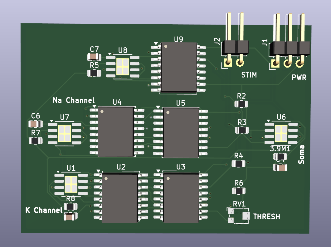
This repository contains the design, simulation, and manufacturing files for an analog computational hardware that physically models the Hodgkin-Huxley (HH) biological neuron. The primary objective is to transition neuro-biophysical concepts from theoretical mathematics into a tangible engineering prototype.
Instead of utilizing microprocessors or algorithmic software to approximate the differential equations, this circuit solves the time and voltage-dependent variables ($V, m, h, n$) in real-time using the inherent physical properties of electrons, capacitors, and non-linear analog multipliers.
The electronic component values in this design are strictly derived from the morphological data of a real biological cell, utilizing foundational physics principles rather than hypothetical values.
By multiplying the universal specific membrane capacitance ($1\ \mu F / cm^{2}$) and specific channel conductances by the actual surface area of the 1-10-8 neuron, the following hardware parameters were calculated and implemented in the circuit:
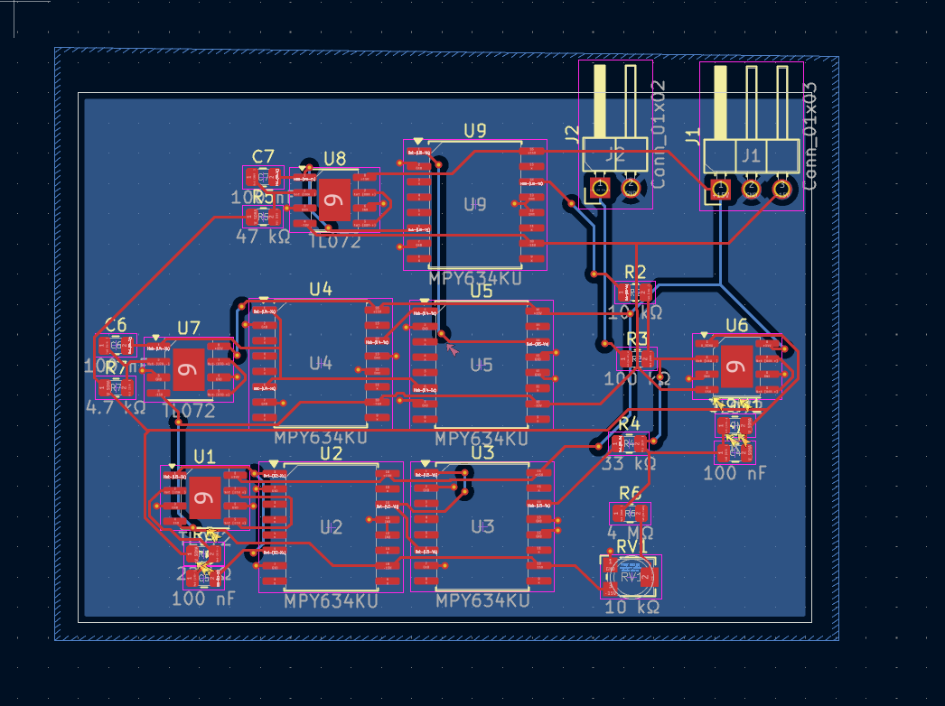
The system is designed on a 2-layer Printed Circuit Board (PCB) using KiCad, featuring an unbroken ground plane on the bottom layer to ensure signal integrity for the analog pathways. Trace widths are constrained to 0.25 mm with 0.20 mm clearances to accommodate the dense IC placement.
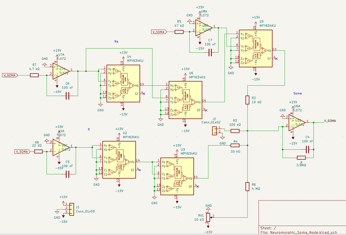
The architecture is divided into three core functional blocks:
Prior to hardware manufacturing, the extracted parameters were simulated in two distinct environments to verify the mathematical model against the electronic implementation.
The standard HH differential equations were solved using numerical integration to establish the baseline biological response. Under a 0.2 nA stimulus, the mathematical model exhibits precise spiking behavior.
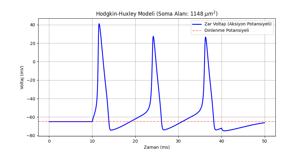
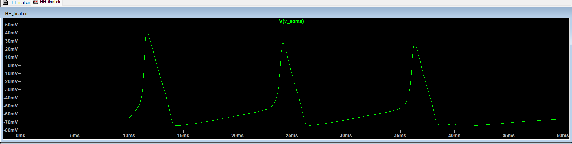
The physical hardware schematic was simulated in LTspice. The resulting transient analysis waveforms confirm that the analog components successfully replicate the action potentials, matching the mathematical ground truth and proving the viability of the physical circuit.
/hardware: Contains KiCad PCB design files and LTspice simulation models./simulation: Contains the Python script (hh_model.py) for the numerical ground truth./images: Renderings and plots used in this documentation.1-10-8_Neuromorpho.md: Detailed mathematical proofs and parameter conversion calculations.| Qty | Value | Footprint | References |
|---|---|---|---|
| 5 | MPY634KU | Package_SO:SOIC-16W_7.5x10.3mm_P1.27mm | U2, U3, U4, U5, U9 |
| 4 | 100 nF | Capacitor_SMD:C_0805_2012Metric | C4, C5, C6, C7 |
| 4 | TL072 | Package_SO:SOIC-8-1EP_3.9x4.9mm_P1.27mm_EP2.62x3.51mm | U1, U6, U7, U8 |
| 1 | 10 kΩ | Potentiometer_SMD:Potentiometer_Bourns_TC33X_Vertical | RV1 |
| 1 | 10 kΩ | Resistor_SMD:R_0805_2012Metric | R2 |
| 1 | 100 kΩ | Resistor_SMD:R_0805_2012Metric | R3 |
| 1 | 22 kΩ | Resistor_SMD:R_0805_2012Metric | R8 |
| 1 | 33 kΩ | Resistor_SMD:R_0805_2012Metric | R4 |
| 1 | 4 MΩ | Resistor_SMD:R_0805_2012Metric | R6 |
| 1 | 4.7 kΩ | Resistor_SMD:R_0805_2012Metric | R7 |
| 1 | 47 kΩ | Resistor_SMD:R_0805_2012Metric | R5 |
| 1 | Conn_01x02 | Connector_PinHeader_2.54mm:PinHeader_1x02_P2.54mm_Horizontal | J2 |
| 1 | Conn_01x03 | Connector_PinHeader_2.54mm:PinHeader_1x03_P2.54mm_Horizontal | J1 |
| 1 | R | Resistor_SMD:R_0805_2012Metric | 3.9M1 |
ohmtech-rdi/eurorack-blocks
Software to Hardware Prototyping for Eurorack using C++, Max/Gen~ or Faust

ctag-fh-kiel/ctag-tbd
CTAG TBD >>to be determined<< an extendible open source Eurorack sound module

plinkysynth/plinky_public
a public release of the plinky sw and hw


matthewcieplak/super-sixteen
Code and schematics for the Super Sixteen Eurorack sequencer

mzuelch/CATs-Eurosynth
Analog Synth Eurorack Modules

StoneRose35/cortexguitarfx
guitar effects processor implemented on various arm cortex platforms
It measures 60.5 × 43.8 mm and has 2 copper layers, 1.6 mm thick.
24 parts, built around the MPY634KU and TL072. The full list of its parts is on this page, with links to each part's symbol and footprint where PCBKit's library has them.
From the aliihsan1913/Analog-HH-Neuron repository on GitHub, at the commit this page was made from: the board is Hardware/Kicad/Neuromorphic_Soma_Node.kicad_pcb and its schematic Hardware/Kicad/Neuromorphic_Soma_Node.kicad_sch. PCBKit opens the board in the browser, with nothing to install.
Its repository publishes it under the MIT licence: you may reuse it on that licence's terms (keep the author's notice, and for a copyleft licence share your changes alike).