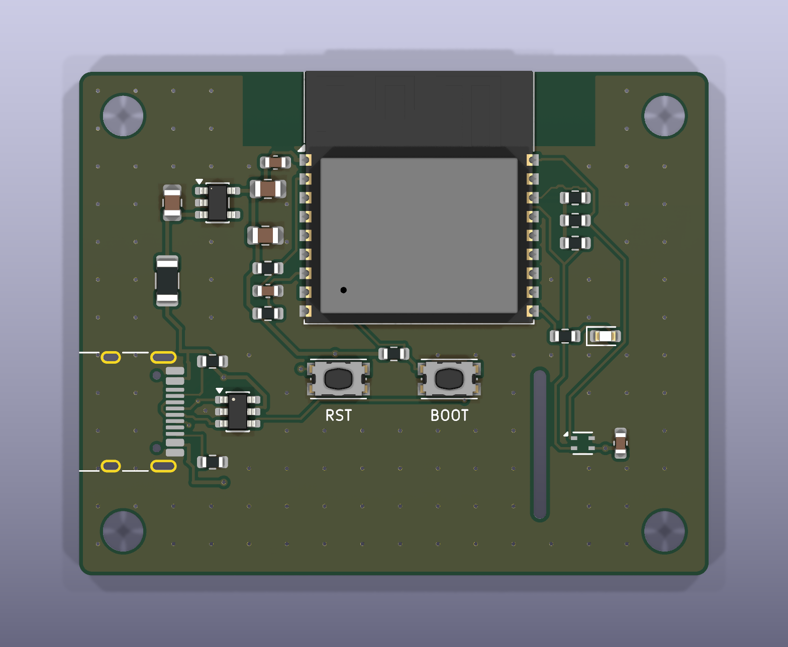
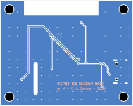
Esp32c3-sensor node is an open-source printed circuit board by Alexden28, from the Alexden28/esp32c3-sensor-node-pcb repository on GitHub, published under the MIT licence. It is a 2-layer board of 50 × 40 mm with 28 parts on 26 nets, routed with 179 tracks and 137 vias.
It is built around the ESP32-C3-WROOM-02-H4, SHT40-AD1B-R2 and AP2112K-3.3, with the USBLC6-2SC6 among its other parts. Its parts include 9 resistors, 6 capacitors, 4 ICs, 2 switches and 1 diode. It belongs with the sensors and measurement and home automation and IoT boards and the ESP32 and RISC-V boards of this library.
A 50 × 40 mm, 2-layer Wi-Fi/BLE temperature and humidity sensor board, powered and programmed
over USB-C. It carries an ESP32-C3-WROOM-02 module and a Sensirion SHT40 sensor, plus USB-C
input protection and a 3.3 V LDO. The schematic and the PCB are both generated from one Python
description (scripts/design.py) through KiCad's file formats and pcbnew API, routed with
Freerouting and verified with KiCad's own checks:
0 errors, 0 unconnected items. 4 warnings: footprint silkscreen of the edge-mounted USB-C and module runs past the board edge and is clipped by the fab (docs/drc.json)
Schematic ↔ PCB parity
0 differences
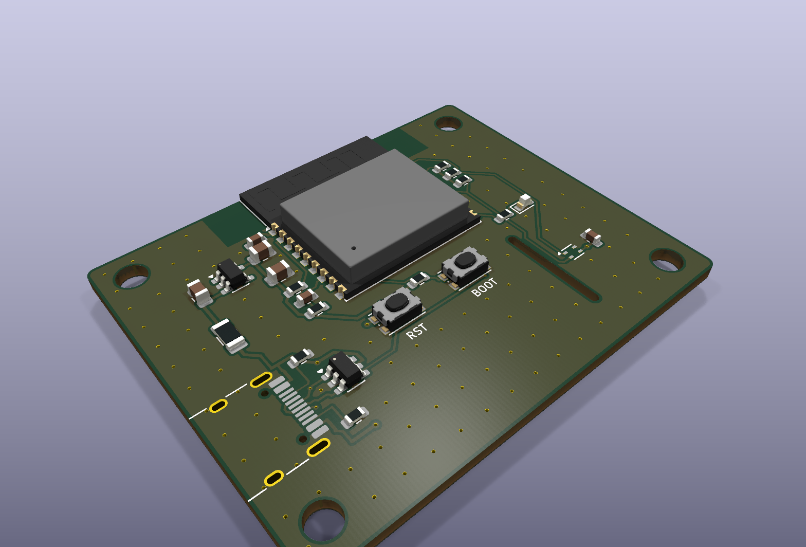
Top (3D render)
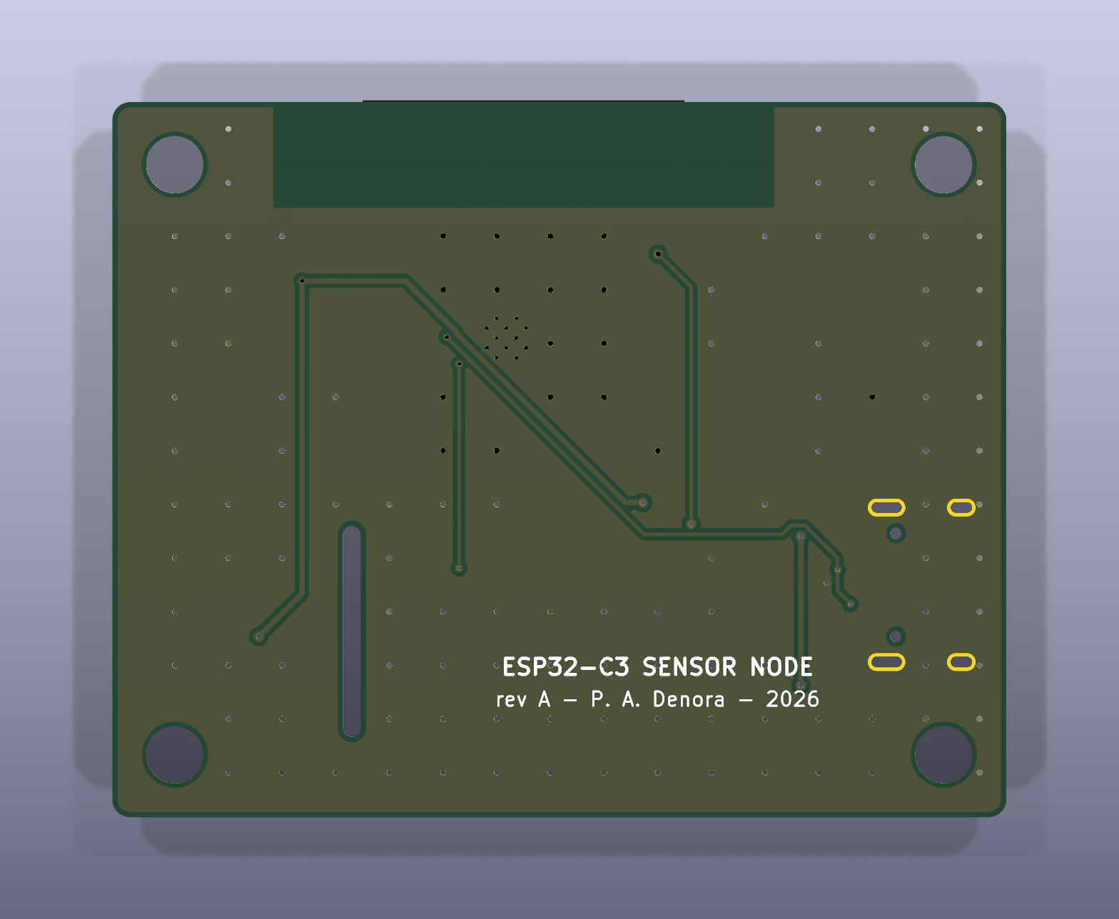
Bottom
The board fits the 3D-printed enclosure in
freecad-parametric-parts. That enclosure is
generated from this board's placement, and its pipeline checks the base and lid for interference
against the STEP model exported from this PCB.
J1 HRO TYPE-C-31-M-12, R1/R2 5.1 kΩ, U1 USBLC6-2SC6, F1 500 mA PTC
5.1 kΩ CC pull-downs advertise a USB 2.0 sink; both D+/D− pin pairs are tied for plug reversibility; ESD array right behind the connector
3.3 V supply
U2 AP2112K-3.3, C1/C2 10 µF
600 mA LDO, which covers the ESP32-C3 Wi-Fi TX peaks (~350 mA)
MCU
U3 ESP32-C3-WROOM-02, C3 10 µF + C4 100 nF
Native USB Serial/JTAG on IO18/IO19, so no USB-UART bridge is needed
Reset / boot
R3 10 kΩ + C5 1 µF on EN, SW1 RESET, SW2 BOOT on IO9
Strapping pins per Espressif: IO9 has a pull-up (low at reset = download mode), IO8 and IO2 are pulled high
Status
R6 1 kΩ + green LED on IO10
~1.3 mA
Sensor
U4 SHT40-AD1B, C6 100 nF, R7/R8 4.7 kΩ
I²C at 0x44 on IO0 (SDA) / IO1 (SCL)
Layout
2 layers, 1.6 mm: signals mostly on F.Cu, a GND pour on both layers tied together by
125 stitching vias, 179 track segments (343 mm), 12 signal vias.
Antenna: the module sits on the top edge with its antenna over a copper-free keep-out
(Espressif's recommended clearance, taken from the footprint's rule area).
Thermal isolation of the sensor: the SHT40 sits in the corner furthest from the LDO, behind a
1 mm milled slot that blocks heat conduction from the module. The footprint keeps copper out from
under the sensing die.
USB: the D+/D− pads interleave on a 0.5 mm pitch (B7 D−, A6 D+, A7 D−, B6 D+), so the USB
net class uses 0.2 mm tracks with 0.15 mm clearance and 0.45/0.2 mm vias to cross the pairs.
Net classes (in scripts/project.kicad_pro): Default 0.2 mm, Power 0.3 mm, USB 0.2 mm;
minimum track/space 0.15 mm, minimum drill 0.2 mm (also needed by the module's thermal vias).
This is within standard 2-layer service at JLCPCB and PCBWay.
Reference designators go on the Fab layer to keep the silkscreen clean. RST/BOOT are labelled on
top, and the board name and revision are on the back.
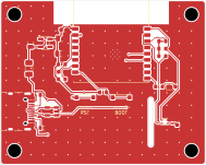
Top copper
Bottom copper (mirrored)
Manufacturing files
fab/ holds everything needed to order the board and have it assembled:
Bill of materials grouped by value/footprint (24 placed parts)
positions_top.csv
Pick-and-place file (all parts on the top side)
esp32c3-sensor-node.step
3D model of the assembled board (used by the enclosure checks)
How it is built
text
scripts/design.py        parts, footprints, pin -> net map, schematic positions, PCB placement
scripts/gen_schematic.py writes the .kicad_sch: symbols embedded from the KiCad 10 libraries, a wire
                         stub + label or power symbol on every pin, no-connect flags on unused pins
scripts/gen_pcb.py       pcbnew API: reads KiCad's own netlist export (so nets and symbol links match
                         the schematic exactly), places footprints, draws the outline and sensor slot,
                         pours GND, exports/imports Specctra for Freerouting, then removes dangling
                         autorouter leftovers and adds GND stitching vias (also one per isolated pour island)
scripts/dsn_skip_nets.py leaves GND to the pours instead of the autorouter
build.sh                 the whole flow + ERC/DRC; retries routing until the board is fully connected
export_fab.sh            Gerbers, drill, BOM, positions, STEP, schematic PDF/SVG, renders
bash
FREEROUTING_JAR=/path/to/freerouting-2.5.0.jar ./build.sh   # regenerate everything (KiCad 10, Java 17+)
./export_fab.sh                                             # outputs only, from the routed board
The KiCad project in hardware/ opens normally in KiCad 10. The project-level library tables point
at the standard ${KICAD10_SYMBOL_DIR} / ${KICAD10_FOOTPRINT_DIR} libraries.
Tools
KiCad 10 (Eeschema / Pcbnew file formats, pcbnew Python API, kicad-cli for ERC/DRC/fab
outputs/3D renders), Freerouting 2.5, Python. Developed with AI-assisted pair programming (Claude Code).
It measures 50 × 40 mm and has 2 copper layers, 1.6 mm thick.
What parts does the Esp32c3-sensor node use?
28 parts, built around the ESP32-C3-WROOM-02-H4, SHT40-AD1B-R2, AP2112K-3.3 and USBLC6-2SC6. The full list of its parts is on this page, with links to each part's symbol and footprint where PCBKit's library has them.
Where can I download the Esp32c3-sensor node KiCad files?
From the Alexden28/esp32c3-sensor-node-pcb repository on GitHub, at the commit this page was made from: the board is hardware/esp32c3-sensor-node.kicad_pcb and its schematic hardware/esp32c3-sensor-node.kicad_sch. PCBKit opens the board in the browser, with nothing to install.
Can I use the Esp32c3-sensor node design in my own project?
Its repository publishes it under the MIT licence: you may reuse it on that licence's terms (keep the author's notice, and for a copyleft licence share your changes alike).
A tiny plug-in board for the rev E phone-companion board. It stands upright in a notch in rev E's sensor end, between the two gas sensor cans, and pokes 4.5 mm out through a slot in the case face, so its tip sits in the…