2 layers76.8 × 100 mm
Project CV
KazimGL/ESP32-PowerIoT-DevBoard
ESP32 battery-powered IoT dev board with Li-ion charging, protection, and sensor support — designed in KiCad
62 parts

 albertoboffi-PERSONAL/fra-clock
A one-off gift PCB designed in KiCad 10: an ESP32 clock with a ring of 180 WS2812B‑2020 LEDs, a photo printed in exposed copper on the front, two Makerverse 8 Ω / 5 W speakers driven by two MAX98357A I²S amplifiers…
Fra clock is an open-source printed circuit board by albertoboffi-PERSONAL, from the albertoboffi-PERSONAL/fra-clock repository on GitHub. It is a 2-layer board of 210 × 297 mm with 428 parts on 262 nets, routed with 3,162 tracks and 488 vias.
It is built around the 74AHCT125D, CH340C and ESP32-WROOM-32E, with the AP2112K-3.3, USBLC6-2SC6 and WS2812B-2020 among its other parts. Its parts include 194 capacitors, 180 diodes, 20 resistors, 7 ICs and 3 transistors. It belongs with the lEDs and displays boards and the ESP32 boards of this library.


A one-off gift PCB designed in KiCad 10: an ESP32 clock with a ring of 180 WS2812B‑2020 LEDs, a photo printed in exposed copper on the front, two Makerverse 8 Ω / 5 W speakers driven by two MAX98357A I²S amplifiers, USB‑C power/programming (CH340C) and an NFC tag area.
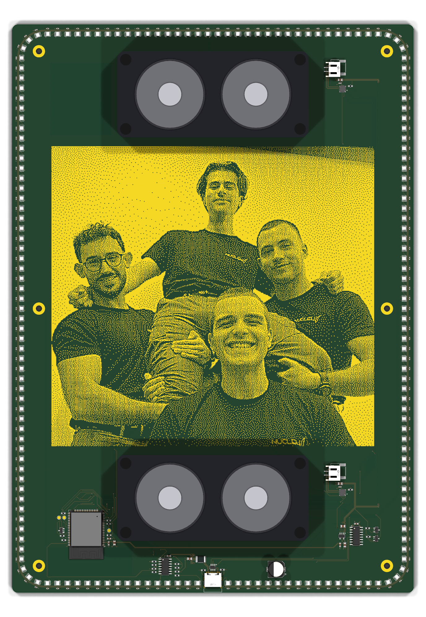
| Board | 2 layers, 210 × 297 mm (A4), R3 corners |
| MCU | ESP32‑WROOM‑32E |
| LEDs | 180 × WS2812B‑2020 (4 chains, 74AHCT125 level shifter) |
| Audio | 2 × MAX98357A → 2 × JST PH (speakers Core Electronics CE08483) |
| Power / USB | USB‑C (HRO TYPE‑C‑31‑M‑12), 2 A PTC, AP2112K‑3.3, USBLC6‑2SC6, CH340C |
| Status | Routed, DRC clean (0 errors, 0 unconnected), Gerber/drill + JLCPCB BOM/CPL generated. Not fabricated yet. |
hardware/                 KiCad project – open hardware/fra_clock.kicad_pro
  fra_clock.kicad_pcb     board
  fra_clock.kicad_sch     root schematic (+ led_ring.kicad_sch sub-sheet)
  fra_clock.pretty/       project footprints (photo art ART_FOTO, speaker outline)
  3d/                     project 3D models (speaker, LCSC/EasyEDA models in lcsc/)
production/
  fra_clock_gerber_jlcpcb.zip   upload this to the fab
  gerber/                 Gerber X2 + Excellon drill (+ drill maps)
  assembly/               JLCPCB BOM and CPL (pick & place)
  preview/                Gerber renders used for the visual check
docs/
  routing-report.md       full design/routing report (Italian)
  checks/                 DRC and verification outputs referenced by the report
  images/                 3D renders
art/
  source/foto.jpeg        original photo
  generated/              dithered bitmap, rectangle list, previews
scripts/ automation used to build the board (see scripts/README.md)production/fra_clock_gerber_jlcpcb.zip (2 layers, 1.6 mm).production/assembly/fra_clock_BOM_JLCPCB.csv and fra_clock_CPL_JLCPCB.csv, then check rotation / pin 1 in the placement preview (SOT‑23/‑5/‑6, SOIC, TQFN, WS2812B‑2020, ESP32 antenna towards the edge, USB‑C, JST, C69 polarity).The NFC tag (NTAG216 sticker) has no footprint and is applied by hand in the keep-out area.
From the repository root, with KiCad 10 (kicad-cli):
KC=/Applications/KiCad/KiCad.app/Contents/MacOS/kicad-cli
$KC pcb drc --refill-zones --schematic-parity --format json --severity-all -o docs/checks/drc_latest.json hardware/fra_clock.kicad_pcb
$KC pcb export gerbers -o production/gerber/ --layers F.Cu,B.Cu,F.Paste,B.Paste,F.Silkscreen,B.Silkscreen,F.Mask,B.Mask,Edge.Cuts --subtract-soldermask --check-zones hardware/fra_clock.kicad_pcb
$KC pcb export drill -o production/gerber/ --format excellon --drill-origin absolute --excellon-units mm --excellon-zeros-format decimal --excellon-oval-format alternate --excellon-separate-th --generate-map --map-format gerberx2 hardware/fra_clock.kicad_pcb
python3 scripts/production/dump_fps.py hardware/fra_clock.kicad_pcb /tmp/fps.json
(cd production/assembly && python3 ../../scripts/production/make_bom_cpl.py /tmp/fps.json)See docs/routing-report.md §5: a ~1035 mm² island of the bottom GND pour around U6/C4 is tied to GND only through top-side bridges; the exposed-pad vias of U101/U102 are not plugged; the Power net class is not assigned (widths are set explicitly on the tracks).
| Qty | Value | Footprint | References |
|---|---|---|---|
| 182 | 100nF | Capacitor_SMD:C_0402_1005Metric | C101, C102, C201, C202, C203, C204, C205, C206, C207, C208, C209, C210, C211, C212, C213, C214 +166 |
| 180 | WS2812B-2020 | LED_SMD:LED_WS2812B-2020_PLCC4_2.0x2.0mm | D201, D202, D203, D204, D205, D206, D207, D208, D209, D210, D211, D212, D213, D214, D215, D216 +164 |
| 8 | 10k | Resistor_SMD:R_0603_1608Metric | R3, R4, R5, R6, R7, R16, R17, R18 |
| 8 | MountingHole_4.3mm_M4_Pad | MountingHole:MountingHole_4.3mm_M4_Pad | H3, H4, H5, H6, H9, H10, H11, H12 |
| 6 | MountingHole_3.2mm_M3_Pad | MountingHole:MountingHole_3.2mm_M3_Pad | H1, H2, H7, H8, H13, H14 |
| 5 | 10uF | Capacitor_SMD:C_0805_2012Metric | C3, C4, C6, C71, C72 |
| 4 | 100nF | Capacitor_SMD:C_0603_1608Metric | C1, C5, C8, C70 |
| 4 | 470 | Resistor_SMD:R_0603_1608Metric | R8, R13, R14, R15 |
| 3 | 33 | Resistor_SMD:R_0603_1608Metric | R10, R11, R12 |
| 3 | TestPoint | TestPoint:TestPoint_Pad_D1.5mm | TP1, TP2, TP3 |
| 2 | 1M | Resistor_SMD:R_0603_1608Metric | R101, R102 |
| 2 | 5.1k | Resistor_SMD:R_0603_1608Metric | R1, R2 |
| 2 | CE08483 | fra_clock:Speaker_Makerverse_CE08483_100x45 | LS1, LS2 |
| 2 | MAX98357A | Package_DFN_QFN:TQFN-16-1EP_3x3mm_P0.5mm_EP1.23x1.23mm | U101, U102 |
| 2 | MMBT3904 | Package_TO_SOT_SMD:SOT-23 | Q1, Q2 |
| 1 | 100k | Resistor_SMD:R_0603_1608Metric | R9 |
| 1 | 1uF | Capacitor_SMD:C_0603_1608Metric | C7 |
| 1 | 22uF | Capacitor_SMD:C_0805_2012Metric | C2 |
| 1 | 2A | Fuse:Fuse_1812_4532Metric | F1 |
| 1 | 2N7002 | Package_TO_SOT_SMD:SOT-23 | Q3 |
| 1 | 470uF | Capacitor_SMD:CP_Elec_8x10 | C69 |
| 1 | 74AHCT125 | Package_SO:SOIC-14_3.9x8.7mm_P1.27mm | U6 |
| 1 | AP2112K-3.3 | Package_TO_SOT_SMD:SOT-23-5 | U1 |
| 1 | ART_FOTO | fra_clock:ART_FOTO | ART1 |
| 1 | CH340C | Package_SO:SOIC-16_3.9x9.9mm_P1.27mm | U5 |
| 1 | ESP32-WROOM-32E | RF_Module:ESP32-WROOM-32E | U3 |
| 1 | SPK_BOT | Connector_JST:JST_PH_S2B-PH-SM4-TB_1x02-1MP_P2.00mm_Horizontal | J102 |
| 1 | SPK_TOP | Connector_JST:JST_PH_S2B-PH-SM4-TB_1x02-1MP_P2.00mm_Horizontal | J101 |
| 1 | USBLC6-2SC6 | Package_TO_SOT_SMD:SOT-23-6 | U2 |
| 1 | USB_C | Connector_USB:USB_C_Receptacle_HRO_TYPE-C-31-M-12 | J1 |
KazimGL/ESP32-PowerIoT-DevBoard
ESP32 battery-powered IoT dev board with Li-ion charging, protection, and sensor support — designed in KiCad


durveshpathak1989/kicad-local-agent
Free local Ollama agent for generating and validating KiCad project files

hpralfi/comfoair-esp32
ESP32-Platine, um Zehnder ComfoAir, StorkAir WHR und Wernig G90 über RS232 in Home Assistant einzubinden (ESPHome, ohne Cloud)

kaorii-ako/Poket
ESP32-S3 Bluetooth MP3 player - custom PCB + 3D-printed case, built from scratch

jonny190/TableLight
A 3D-printable, battery-powered, USB-C rechargeable table lamp in the classic "Poldina" shape - honeycomb disc base, thin stem, down-firing cone shade with a white top - running WLED on an ESP32, with a capacitive touch…


hamzaa-exe/PixelBoard
LED display using Sparkle Motion and a 16x16 NeoPixel matrix. Use WLED software to play awesome animations that are designed for 2D matrices.
It measures 210 × 297 mm and has 2 copper layers, 1.6 mm thick.
428 parts, built around the 74AHCT125D, CH340C, ESP32-WROOM-32E and AP2112K-3.3. The full list of its parts is on this page, with links to each part's symbol and footprint where PCBKit's library has them.
From the albertoboffi-PERSONAL/fra-clock repository on GitHub, at the commit this page was made from: the board is hardware/fra_clock.kicad_pcb and its schematic hardware/fra_clock.kicad_sch. PCBKit opens the board in the browser, with nothing to install.
Its repository states no licence, so its author keeps all rights: ask albertoboffi-PERSONAL before reusing the design.