


4 layers78 × 56 mm

 ajefferies2/t1conv
100BASE-T1 ↔ 100BASE-TX media converter + dual CAN FD/USB adapter on one board.
T1conv is an open-source printed circuit board by ajefferies2, from the ajefferies2/t1conv repository on GitHub. It is a 4-layer board of 100 × 60 mm with 125 parts on 132 nets, routed with 787 tracks and 198 vias.
It is built around the STM32G0B1CET6, TCAN1042HGVDRBRQ1 and DP83TC811RWRNDRQ1, with the AP63203QWU, DP83822IRHBR and AQY212GHAX among its other parts. Its parts include 47 capacitors, 34 resistors, 11 ICs, 6 diodes and 6 connectors. It belongs with the STM32 boards of this library.


100BASE-T1 ↔ 100BASE-TX media converter + dual CAN FD/USB adapter on one board.
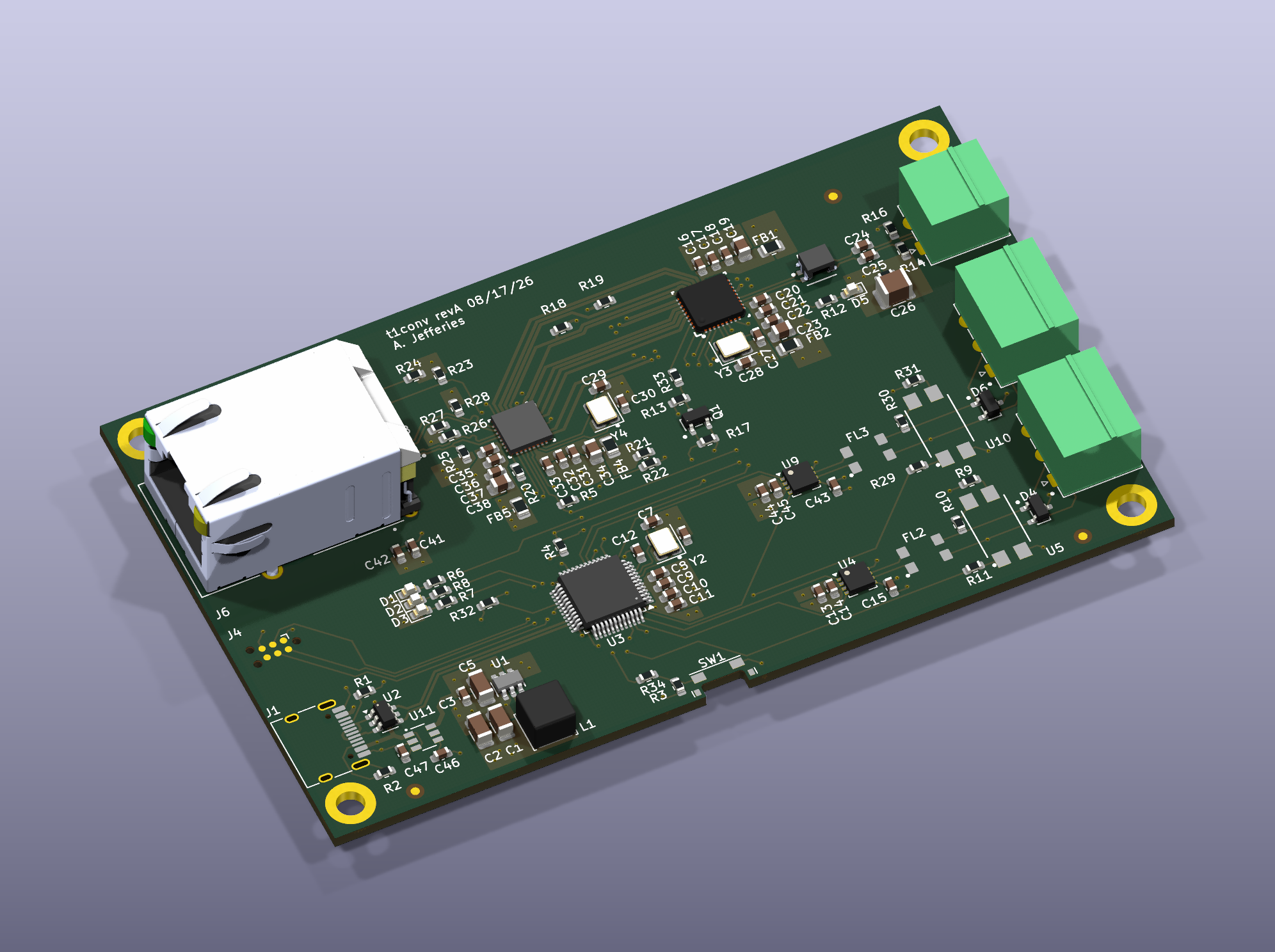
Rendered from the saved hardware on 4 November 2026. Some footprints, including the USB connector, CAN chokes, and PhotoMOS relays, have no 3D model; use the assembly drawing to review their placement.
No Gerber viewer is needed. These exports come from the KiCad sources in this repository; the PDFs and SVGs support zooming into component labels and routing.
| View | What to look at |
|---|---|
| Complete schematic PDF | Six sheets: system, power, MCU, CAN, T1, Ethernet |
| Top assembly drawing · SVG | Component outlines, references, and connector placement |
| Bottom assembly drawing · SVG | Underside, viewed from below |
| Four copper layers PDF | One page per layer, all viewed from above |
| Top 3D view · Bottom 3D view | Board orientation and mechanical overview |
| KiCad project · PCB | Editable design sources |
The DP83TC811 and DP83822 pass Ethernet data directly between them over RGMII. The STM32G0B1 handles PHY setup and the two CAN FD channels, each with a TCAN1042 transceiver. I'm planning to use gs_usb for CAN over USB.
Each CAN channel has switchable termination: two 60.4 Ω resistors and a PhotoMOS relay. CAN and USB share ground, so this is not an isolated adapter.
USB-C supplies power through a TPS22918 soft-start load switch and provides the USB connection. There are SWD pads and a BOOT button for programming and recovery through the STM32's ROM bootloader.
MAC[2:0] = 101).
The DP83822 also delays its incoming TX clock by default
(0x17[11] = 0, 0x17[12] = 0). Each PHY handles the delay on its own input.Complete schematic PDF · KiCad schematics. Click each image for a zoomable SVG.


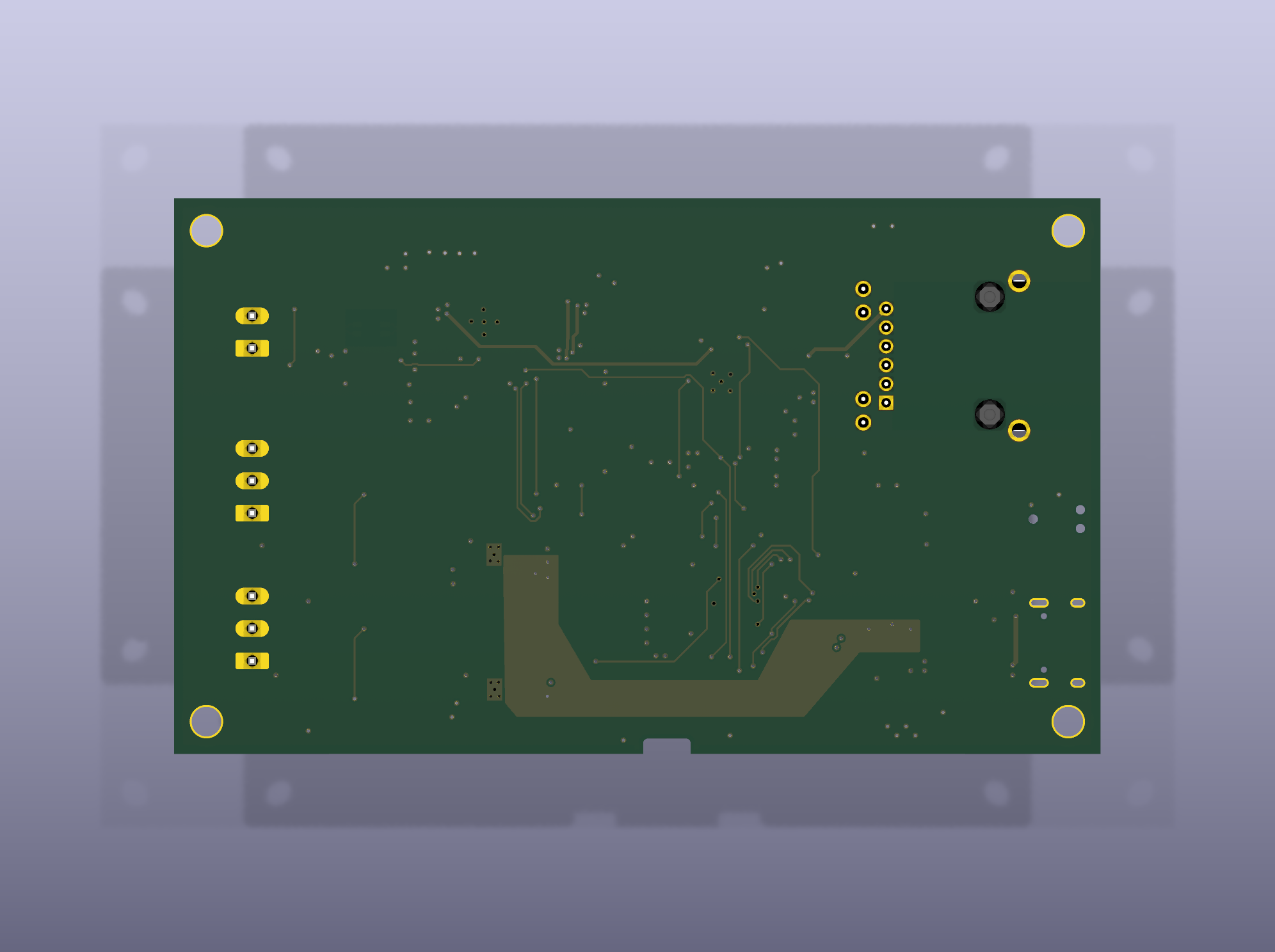
Bottom assembly PDF. Both underside views are mirrored relative to the copper-layer plots below.
The board is four layers, ~1.6 mm thick. The planned stackup is JLC04161H-7628. All copper-layer pictures are viewed from above, including B.Cu, so features line up between layers. Click an image for its vector version.
| Layer | Use |
|---|---|
| L1: F.Cu | Components, signals, and local copper pours |
| L2: In1.Cu | Ground plane |
| L3: In2.Cu | Power planes: 3.3 V, USB VBUS, and Ethernet AVD33 |
| L4: B.Cu | Signals and local copper pours |


This is a design-review snapshot, not a manufacturing release. KiCad 10.0.6 checks on 4 November 2026 reported 0 unrouted connections, 4 DRC errors, and 0 ERC errors. The four DRC errors are SW1 copper-to-board-edge clearances. There are also 23 DRC warnings, 15 schematic/PCB parity warnings, and 16 ERC warnings; see the DRC report and ERC report. These checks do not establish hardware functionality or replace bring-up testing. The earlier August Gerber package predates this design and should not be used to manufacture this snapshot.
To regenerate the review exports, use KiCad 10 (including its Python pcbnew
module), Inkscape, and Python 3:
python3 scripts/export-hardware.pyUse --skip-3d to update only the drawings and rule-check reports. Rendering
requires the standard KiCad 3D models and the personal models referenced by
${ATJ_LIB}; missing models do not appear in the 3D views. The drawings use
the symbols and footprints embedded in the design. Exported copper views
refill zones in memory; the script does not save changes to the source board.
Source SHA-256 hashes identify the saved
hardware used for these exports.
| Qty | Value | Footprint | References |
|---|---|---|---|
| 18 | .1uF | Capacitor_SMD:C_0603_1608Metric | C3, C4, C10, C12, C14, C15, C17, C21, C24, C25, C32, C36, C39, C41, C43, C45 +2 |
| 7 | 1uF | Capacitor_SMD:C_0603_1608Metric | C18, C22, C33, C37, C40, C42, C47 |
| 5 | 470 | Resistor_SMD:R_0603_1608Metric | R6, R7, R8, R12, R24 |
| 4 | 10nF | Capacitor_SMD:C_0603_1608Metric | C16, C20, C31, C35 |
| 4 | 10uF | Capacitor_SMD:C_0805_2012Metric | C19, C23, C34, C38 |
| 4 | 12pF | Capacitor_SMD:C_0603_1608Metric | C6, C7, C29, C30 |
| 4 | 1k@100MHz | Resistor_SMD:R_0805_2012Metric | FB1, FB2, FB4, FB5 |
| 4 | 2.49k | Resistor_SMD:R_0603_1608Metric | R5, R18, R19, R23 |
| 4 | 49.9 | Resistor_SMD:R_0603_1608Metric | R25, R26, R27, R28 |
| 4 | 60.4 | Resistor_SMD:R_0603_1608Metric | R9, R10, R30, R31 |
| 4 | LED | LED_SMD:LED_0603_1608Metric | D1, D2, D3, D5 |
| 3 | 4.7uF | Capacitor_SMD:C_0603_1608Metric | C11, C13, C44 |
| 2 | 100k | Resistor_SMD:R_0603_1608Metric | R14, R17 |
| 2 | 10k | Resistor_SMD:R_0603_1608Metric | R3, R4 |
| 2 | 22pF | Capacitor_SMD:C_0603_1608Metric | C27, C28 |
| 2 | 22uF | Capacitor_SMD:C_1206_3216Metric | C1, C2 |
| 2 | 25MHz | passive:Crystal_SMD_3225-4Pin_3.2x2.5mm | Y3, Y4 |
| 2 | 2k | Resistor_SMD:R_0603_1608Metric | R15, R16 |
| 2 | 330 | Resistor_SMD:R_0603_1608Metric | R11, R29 |
| 2 | 5.1k | Resistor_SMD:R_0603_1608Metric | R1, R2 |
| 2 | AQY212GHA | ic:AQY212GHA | U5, U10 |
| 2 | PESD2CAN | ic:SOT-23 | D4, D6 |
| 2 | PhoenixMC_1x03 | connector:PhoenixContact_MC_1,5_3-G-3.5_1x03_P3.50mm_Horizontal | J3, J5 |
| 2 | SRF4532-510Y | passive:SRF4532 | FL2, FL3 |
| 2 | TCAN1042HGVDRBRQ1 | ic:TCAN1042_VSON8 | U4, U9 |
| 1 | 08B0-1X1T-06-F | connector:08B0-1X1T-06-F | J6 |
| 1 | 1.96k | Resistor_SMD:R_0603_1608Metric | R22 |
| 1 | 10uF | Capacitor_SMD:C_1206_3216Metric | C5 |
| 1 | 10uH | passive:SWPA5040 | L1 |
| 1 | 16MHz | passive:Crystal_SMD_3225-4Pin_3.2x2.5mm | Y2 |
| 1 | 1k | Resistor_SMD:R_0603_1608Metric | R34 |
| 1 | 2.2k | Resistor_SMD:R_0603_1608Metric | R33 |
| 1 | 270 | Resistor_SMD:R_0603_1608Metric | R13 |
| 1 | 4.7k | Resistor_SMD:R_0603_1608Metric | R32 |
| 1 | 4.7nF | Capacitor_SMD:C_1210_3225Metric | C26 |
| 1 | 4.7nF | Capacitor_SMD:C_0603_1608Metric | C46 |
| 1 | 4.87k | Resistor_SMD:R_0603_1608Metric | R20 |
| 1 | 6.2k | Resistor_SMD:R_0603_1608Metric | R21 |
| 1 | ACT1210L-201 | passive:ACT1210L_3225 | FL1 |
| 1 | AO3400A | ic:SOT-23 | Q1 |
| 1 | AP63203QWU | ic:AP63203_TSOT26 | U1 |
| 1 | Conn_ARM_SWD_TagConnect_TC2030-NL | Connector:Tag-Connect_TC2030-IDC-NL_2x03_P1.27mm_Vertical | J4 |
| 1 | DP83822 | ic:DP83822_RHB0032B | U7 |
| 1 | DP83TC811R | ic:DP83TC811R_RND0036A | U6 |
| 1 | PhoenixMC_1x02 | connector:PhoenixContact_MC_1,5_2-G-3.5_1x02_P3.50mm_Horizontal | J2 |
| 1 | STM32G0B1CET6 | ic:STM32G0B1_LQFP48 | U3 |
| 1 | SW_Push | passive:SW_Push_Panasonic_EVQP4_EdgeMount | SW1 |
| 1 | TPD4E05U06DQA | ic:TPD4E05U06_DQA0010A | U8 |
| 1 | TPS22918TDBVRQ1 | ic:DBV0006A_N | U11 |
| 1 | TYPE-C-31-M-12 | Connector_USB:USB_C_Receptacle_HRO_TYPE-C-31-M-12 | J1 |
| 1 | USBLC6-2SC6 | ic:SOT-23-6 | U2 |
The 117 most common of 125 parts.
It measures 100 × 60 mm and has 4 copper layers, 1.61 mm thick.
125 parts, built around the STM32G0B1CET6, TCAN1042HGVDRBRQ1, DP83TC811RWRNDRQ1 and AP63203QWU. The full list of its parts is on this page, with links to each part's symbol and footprint where PCBKit's library has them.
From the ajefferies2/t1conv repository on GitHub, at the commit this page was made from: the board is hw/t1conv.kicad_pcb and its schematic hw/Can.kicad_sch. PCBKit opens the board in the browser, with nothing to install.
Its repository states no licence, so its author keeps all rights: ask ajefferies2 before reusing the design.


um-kiho/ti_radar
AWR6843AOP (Antenna-on-Package) 60GHz FMCW 레이더를 이용한 존재 감지(Presence Detection) 시스템입니다. 내장 ARM Cortex-R4F MCU + C674x DSP에서 신호 처리 및 존재 판정을 수행하고, UART로 결과를 출력합니다.

v-cu/dpf-load-monitor-wide
ESP32-P4 diagnostic display for VAG diesels — live DPF and engine data over CAN (UDS) on a 3.19" ultra-wide AMOLED. Firmware, KiCad files, BOM and 3D enclosure.

motor-and-motion-control-lab/mmlab-12PhaseDrive-388Slave
PCB Electronics for Humanoid Robots and Bearingless Motor Systems

thomas-montano/Radio_Puck
Small STM32 based ethernet connected radio puck capable of full duplex transmit and receive as well as dual RX or dual TX. Capable of rates up to 1 Mbps and completely configurable for many kinds of different modes.

misko/prompt2device
The separate vNext PCB skill and orchestrator package is available alongside the reference workflow below; existing projects keep their accepted toolchain until an explicit migration.

ehntoo/100base-t1-converter
This project provides a media converter for connecting 100Base-TX ethernet to 100Base-T1 (Automotive Ethernet) networks, using an NXP TJA1101 PHY.