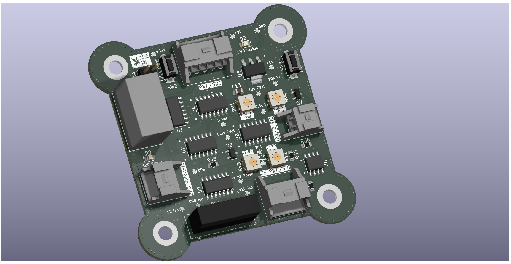
BSPD is an open-source printed circuit board by AditeyaDC, from the AditeyaDC/BSPD repository on GitHub, published under the MIT licence. It is a 2-layer board of 63.3 × 63.3 mm with 130 parts on 72 nets, routed with 930 tracks and 631 vias.
It is built around the LDL1117S50R, BAT42W and TC33X-2-103E, with the 2N7002K, DMG2305UX-7 and BC856BS among its other parts. Its parts include 59 resistors, 13 capacitors, 9 diodes, 8 ICs and 7 transistors.
BSPD RZ-XX6-C/E — Brake System Plausibility Device
Ashwa Racing 27
Designed by Aditeya Sarkar
What is a BSPD?
The Brake System Plausibility Device is a mandatory safety circuit in FSAE/Formula Student vehicles. Its job is to cut power to the motor (via the Shutdown Circuit / SDC) if the driver simultaneously applies heavy braking and demands significant throttle — a condition that should never happen during normal operation and indicates either a pedal fault or a stuck throttle.
This design targets the FSG CV+EV rules (with CV mode support via a jumper) and is built entirely out of discrete analog logic — no microcontroller involved.
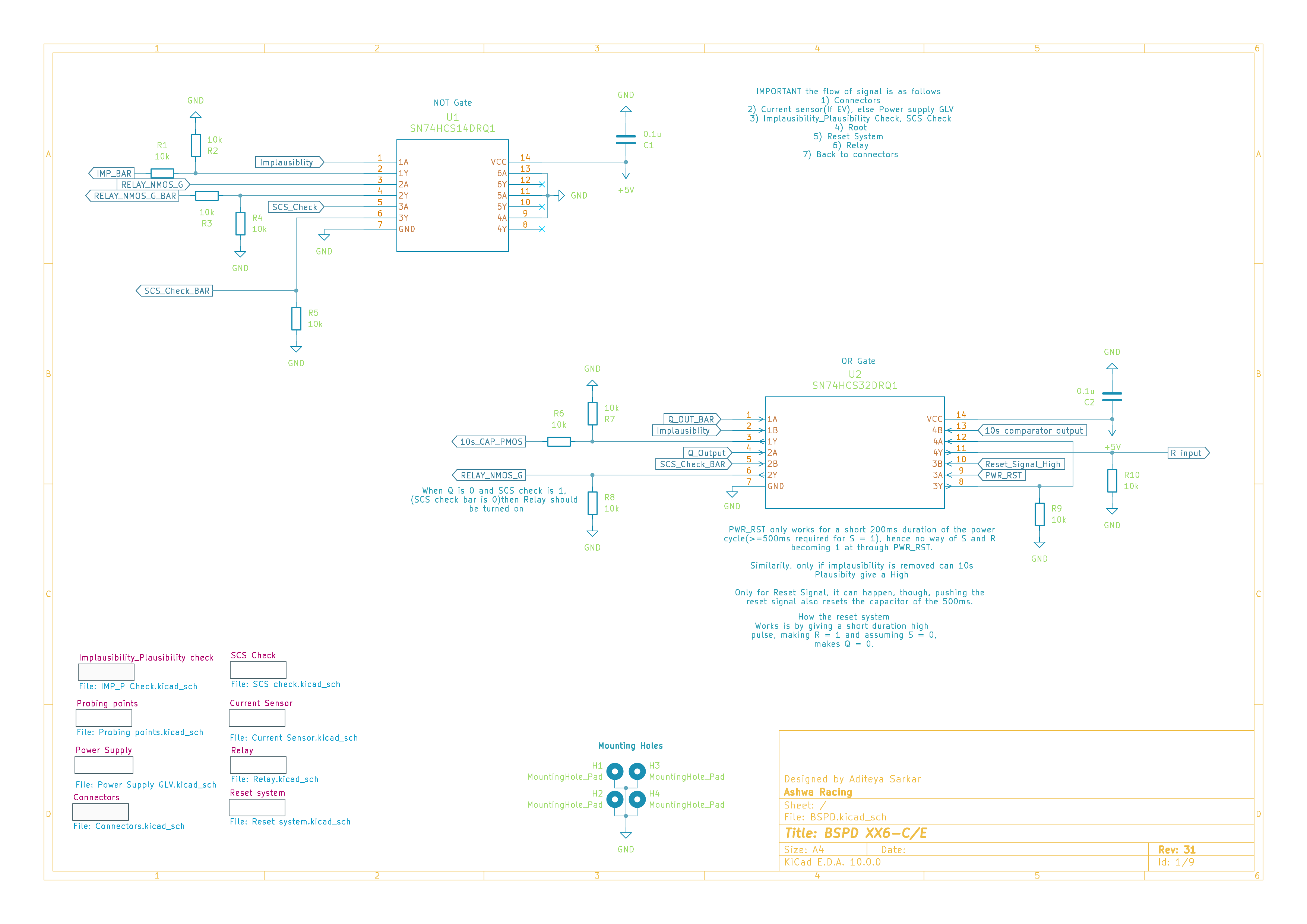
Signal flow as annotated in the schematic (Sheet 1/9)
Schematic Overview
The top-level sheet ties everything together. The core logic sits around a SN74HCS14DRQ1 (Schmitt-trigger inverter, U1) and a SN74HCS32DRQ1 (OR gate, U2), with the relay controlled by a NMOS gate driven off RELAY_NMOS_G_BAR.
Subsystems
1. Power Supply
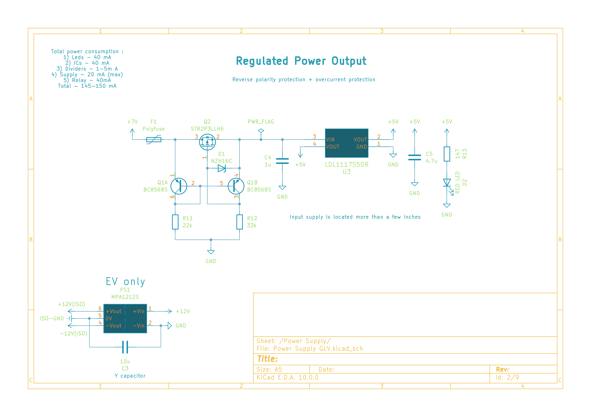
Input is +7V from the car's GLV (Grounded Low Voltage) supply. The board generates a regulated +5V rail using an LDL1117S50R LDO. Protection is handled by:
F1 — Polyfuse for overcurrent
Q2 (STR2P3LLH6) — P-channel MOSFET for reverse polarity protection, driven by a BC856BS transistor pair (Q1A/Q1B)
D1 (NZH16C) — Zener clamp
For EV operation, isolated ±12V rails are generated via an MPA1212S DC-DC isolator (PS1), referenced to ISO-GND, with a Y-capacitor (C3, 10µF) for common-mode filtering.
Total board power budget: ~145–150mA (LEDs 40mA + ICs 40mA + dividers ~5mA + relay 40mA + misc).
2. Implausibility & Plausibility Check
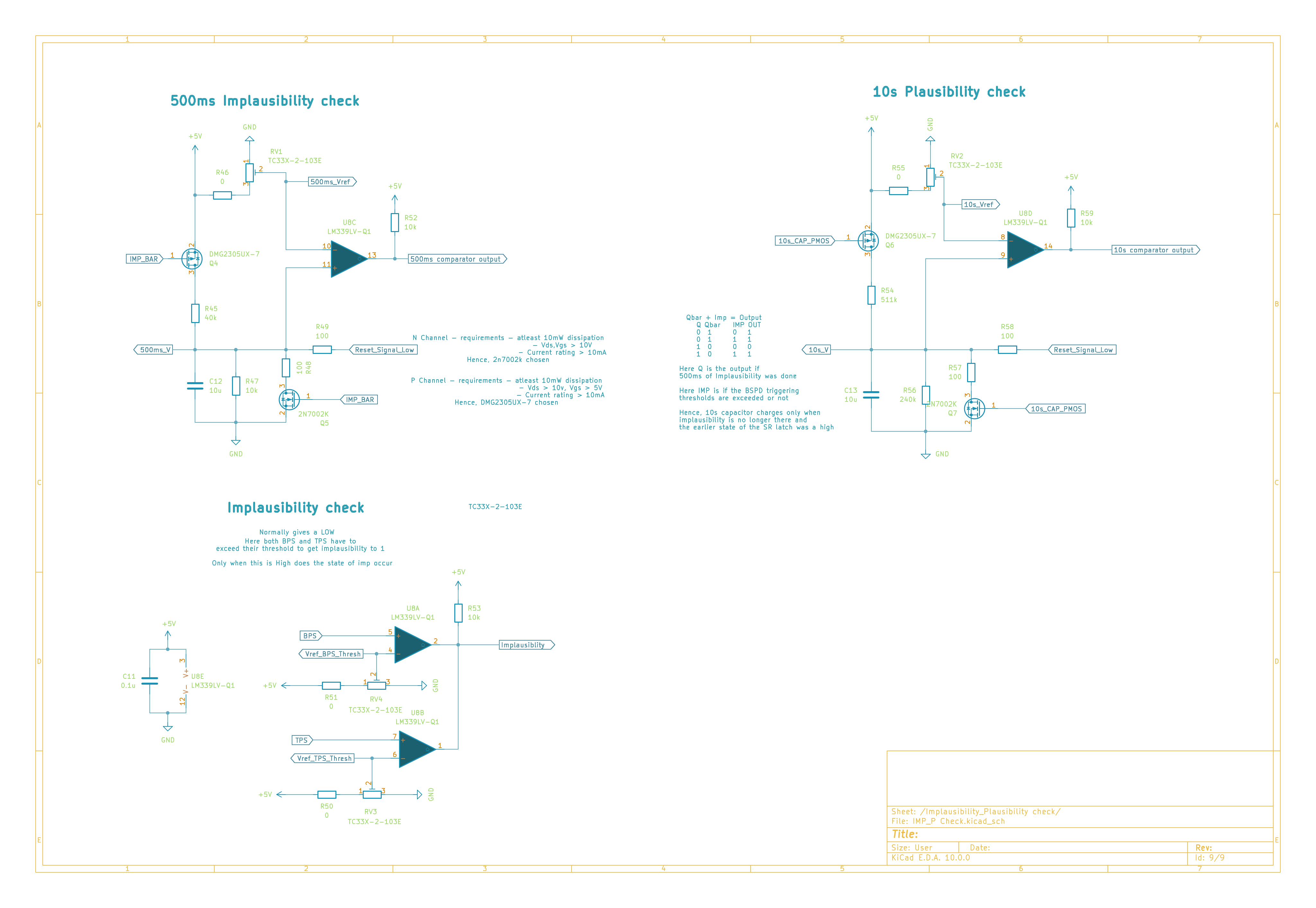
This is the heart of the BSPD logic. Three comparator circuits run in parallel:
Implausibility Check (bottom-left, Sheet 9)
Uses TC33X-2-103E references and LM339LV-Q1 comparators
Both BPS (brake pressure) and TPS (throttle position) must exceed their respective thresholds simultaneously to flag implausibility
Output: Implausibility signal (HIGH = fault)
500ms Implausibility Timer (top-left, Sheet 9)
Uses a DMG2305UX-7 complementary MOSFET pair to charge/discharge a capacitor (C12, 10µF + C13) at a controlled rate
When implausibility is sustained for >500ms, 500ms comparator output goes HIGH
The DWC2305UX-7 N-channel requirements: Vth ~1V, Ids up to 10mA → 2N7002K used
The P-channel: Vth ~−1V, Ids ~10mA → same DWC2305UX-7 (check datasheet for exact variant)
10s Plausibility Timer (top-right, Sheet 9)
Similar RC-based timing circuit; capacitor (C13) only charges when implausibility is active
Output: 10s comparator output — used to latch the fault via the SR latch if the 10s window is exceeded
Reset_Signal_Low can discharge the cap and reset state
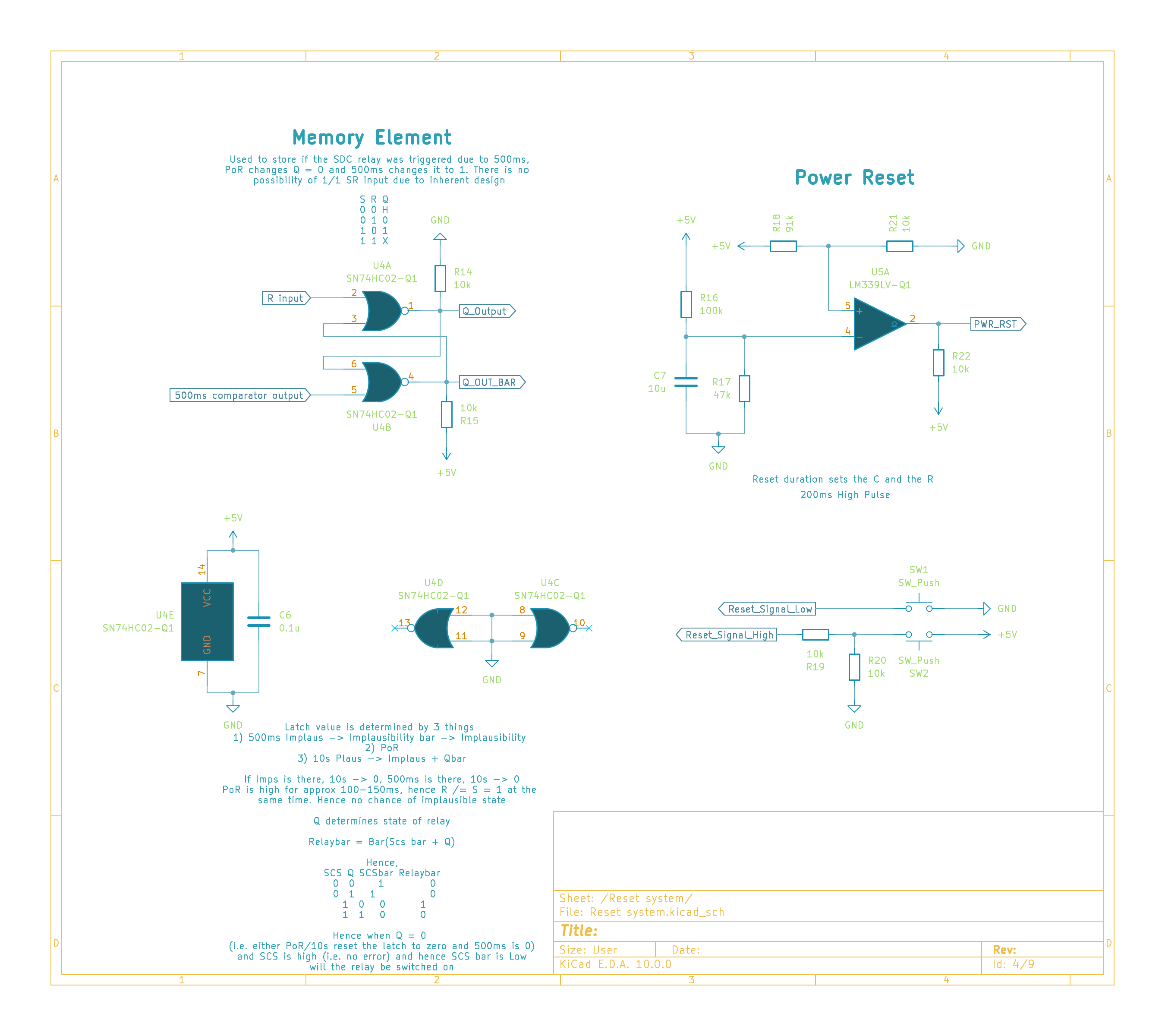
3. Memory Element (SR Latch) + Power Reset
SR Latch (Sheet 4, left)
Built from SN74HC02-Q1 NOR gates (U4A/U4B):
S (500ms)
R
Q
0
0
Hold
0
1
0
1
0
1
Q drives Q_Output and Q_OUT_BAR. The relay state is: Relaybar = NOR(SCS_bar, Q).
So the SDC relay opens (cuts power) only when Q = 0 and SCS_bar is LOW — i.e., no fault and no short circuit detected.
Power-on Reset (Sheet 4, right)
Uses an LM339LV-Q1 comparator (U5A) with R16 (100k), R17 (47k), and C7 (10µF) to generate a ~200ms HIGH pulse on PWR_RST at power-on. This forces the latch into a known state (R = 1 momentarily → Q = 0). Once past the PoR window, R → 0 and normal latch operation resumes.
Two push-buttons (SW1, SW2) provide manual Reset_Signal_High / Reset_Signal_Low for bench testing.
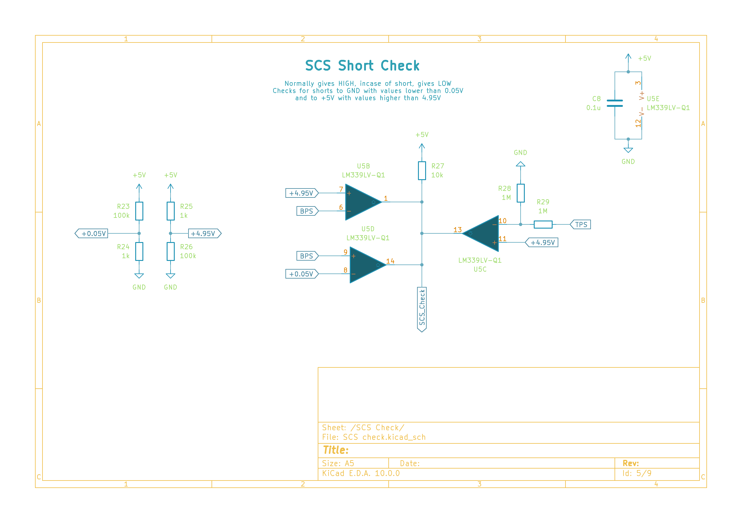
4. SCS Short Circuit Check
The SCS (Short Circuit Safety) check uses LM339LV-Q1 comparators (U5B/U5D/U5C) to detect wiring faults — specifically shorts to GND (<0.05V) or shorts to +5V (>4.95V) on the BPS and TPS lines.
Normally: SCS_Check = HIGH (no fault)
On short detection: goes LOW, which blocks the relay from closing regardless of Q
Thresholds set by 100k/1k voltage divider pairs on each input.
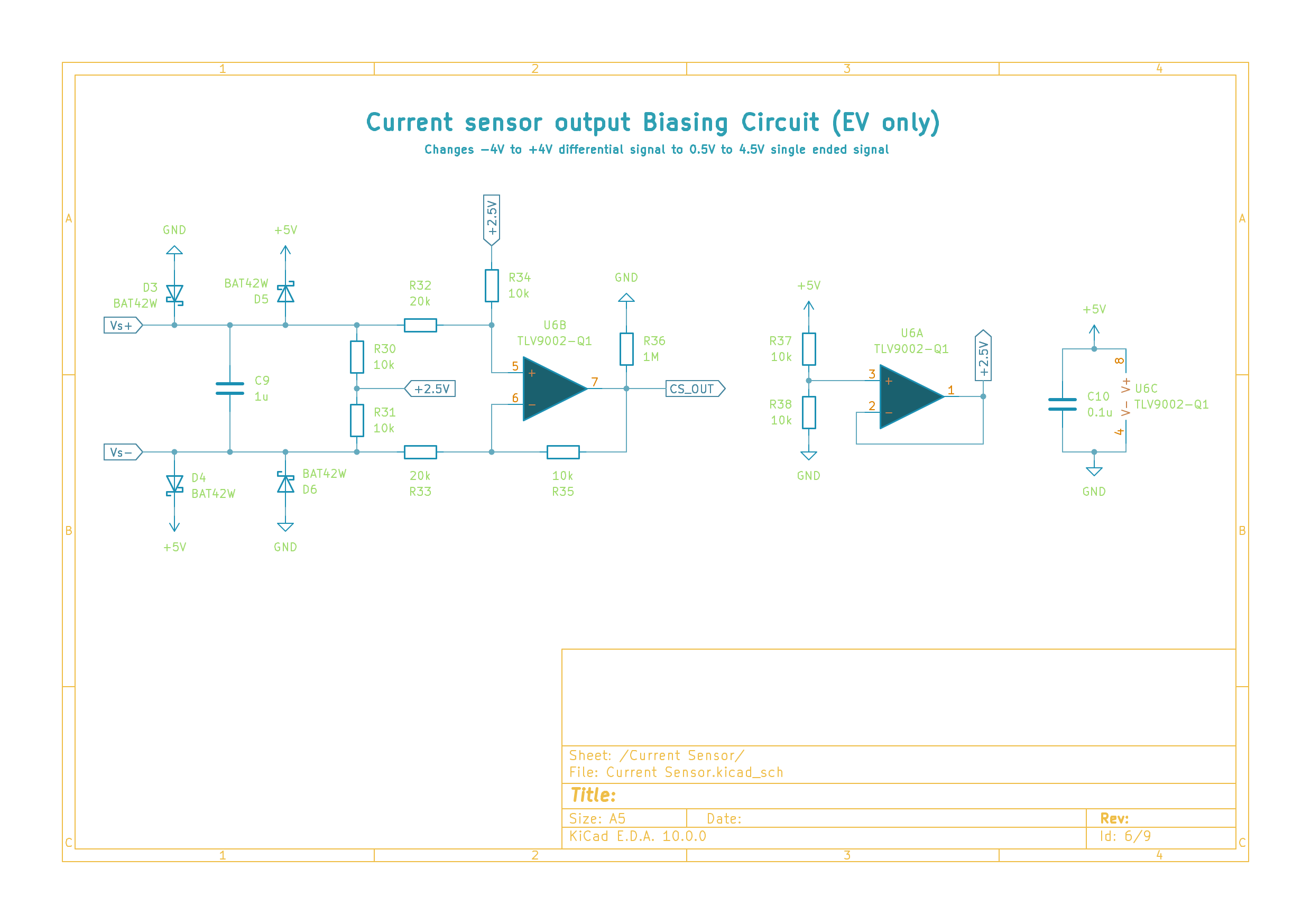
5. Current Sensor (HB0 300) Biasing (EV Only)
The current sensor (external, connected via J3) outputs a differential signal in the ±4V range. Sheet 6 handles the level shift to a 0.5V–4.5V single-ended signal suitable for the comparators.
BAT42W Schottky diodes (D3–D6) clamp Vs+ and Vs− to the 0–5V range
TLV9002-Q1 op-amps (U6A/U6B) in a difference amplifier config with a +2.5V mid-rail reference
Output: CS_OUT → fed into the implausibility comparator as the throttle-side signal in EV mode
A jumper on Sheet 8 allows bypassing this for CV (combustion) mode, where TPS1_IN connects directly
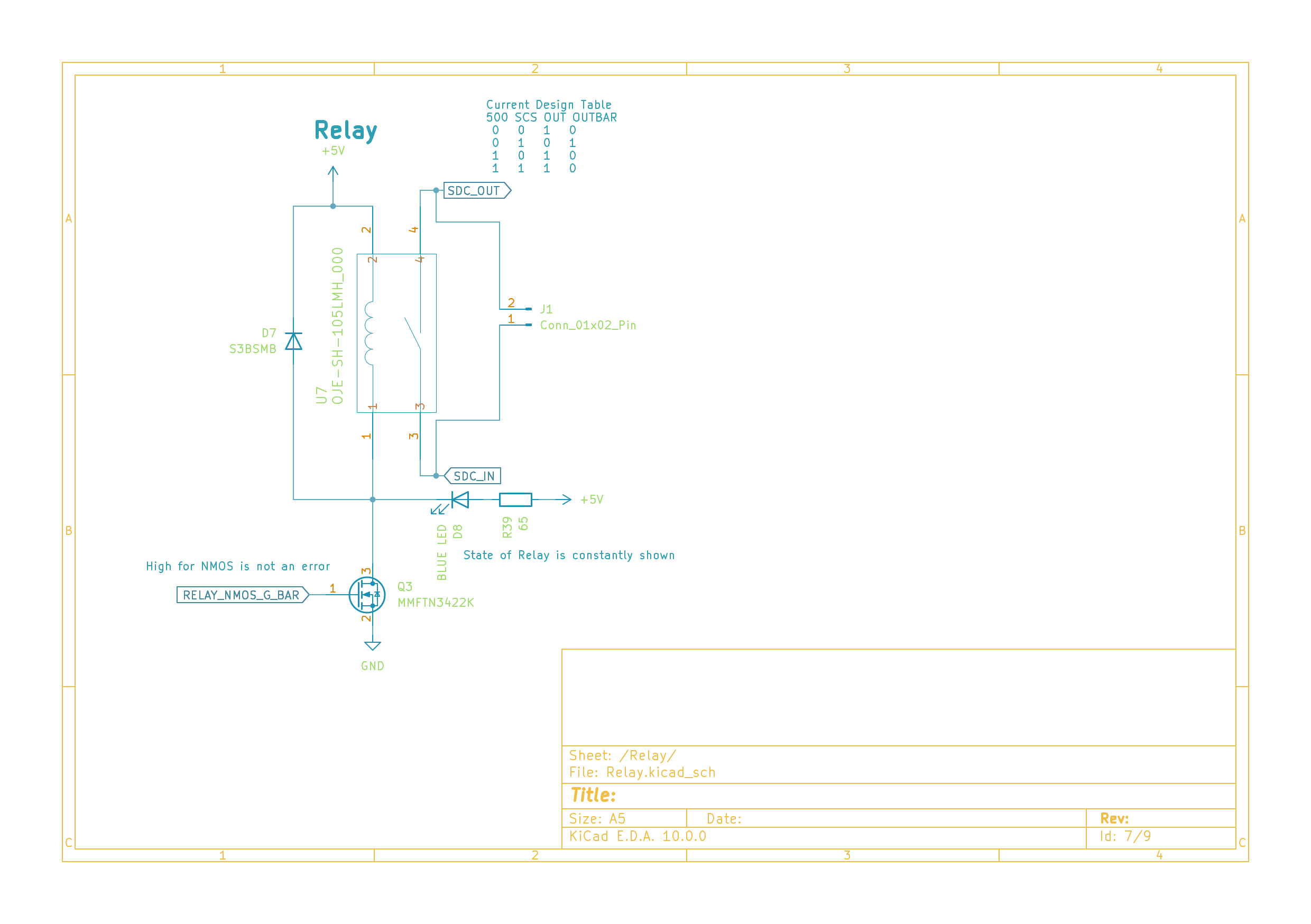
6. Relay
The SDC relay is an OJE-SH-105LMH (U7), driven by an NMOS switch (MMFTN3422K, Q3) on the low side. SDC_OUT drives the relay coil. A S3B5MB diode (D7) provides flyback protection. A blue LED gives constant visual indication of relay state.
7. Connectors
All external signals come through TE Connectivity 1744426-series connectors:
Connector
Signals
J2 (1744426-5)
PWR_FLAG (+7V), GND, +12V, SDC_IN, SDC_OUT
J3 (1744426-4)
+12V(ISO), Vs−, Vs+, −12V(ISO)
J4 (1744426-3)
GND, BPS_IN, +12V
J5 (1744426-2)
TPS1_IN, GND
BPS scaling: R42 (200Ω) + R43 (430Ω) divider sets BPS_SCLD in the 0.88V–4.4V window.
ESD protection on BPS line via ESDCAN01-2BLY (D9).
8. Probing Points
16 dedicated test points for bench validation:
TP
Net
TP
Net
TP1
+12V
TP2
Vref_BPS_Thresh
TP3
+7V
TP4
500ms_Vref
TP5
+5V
TP6
10s_Vref
TP7
GND
TP8
Vref_TPS_Thresh
TP9
+12V ISO
TP10
10s_V
TP11
GND ISO
TP12
Q_Output
TP13
−12V ISO
TP14
500ms_V
TP15
BPS
TP16
TPS
Key ICs
Part
Function
SN74HCS14DRQ1
Schmitt-trigger inverter (signal conditioning)
SN74HCS32DRQ1
OR gate (implausibility logic)
SN74HC02-Q1
NOR gate SR latch (fault memory)
LM339LV-Q1
Quad comparator (thresholds, SCS, power reset)
TLV9002-Q1
Op-amp (current sensor biasing)
LDL1117S50R
5V LDO regulator
MPA1212S
±12V isolated DC-DC (EV)
OJE-SH-105LMH
SDC relay
MMFTN3422K
N-channel MOSFET (relay driver)
DMG2305UX-7
Complementary MOSFET pair (timer charging)
KiCad Version Compatibility
This schematic was designed in KiCad EDA 10.0.0.
If you're on KiCad v9 and need to open these files, a downconverted v9-compatible version is available — reach out or raise an issue. The downconversion removes v10-specific fields (like uuid blocks and certain footprint attributes) that cause parse errors on older installs.
It measures 63.3 × 63.3 mm and has 2 copper layers, 1.6 mm thick.
What parts does the BSPD use?
130 parts, built around the LDL1117S50R, BAT42W, TC33X-2-103E and 2N7002K. The full list of its parts is on this page, with links to each part's symbol and footprint where PCBKit's library has them.
Where can I download the BSPD KiCad files?
From the AditeyaDC/BSPD repository on GitHub, at the commit this page was made from: the board is BSPD.kicad_pcb and its schematic BSPD.kicad_sch. PCBKit opens the board in the browser, with nothing to install.
Can I use the BSPD design in my own project?
Its repository publishes it under the MIT licence: you may reuse it on that licence's terms (keep the author's notice, and for a copyleft licence share your changes alike).
PSM Major Project: A modular smart parking system combining AI (ANPR/OCR), real-time control (Zephyr/STM32), and FPGA-based motor management (LiteX RISC-V SoC), all coordinated via MQTT for seamless access control and…
This is the official repository for the TurboCAN controller board, designed specifically for the Voron AfterBurner toolhead but can also be used on similar toolheads using NEMA17 steppers.
It was decided to go for a design which incorporated an LTE-M module for managinge the node. This gives almost 100% coverage(in Denmark at least!) and high bandwidth for firmware transfers.