

2 layers370.8 × 298.5 mm
8 Bit Computer
The-Invent0r/8-bit-Computer-PCB
These are the KiCAD files for my 8-Bit Computer.
323 parts142

 adhyayan15/full-adder-pcb
A 1-bit full-adder schematic and routed PCB I designed in KiCad during a PCB-design workshop. The design uses discrete 74LS-series logic ICs, switch inputs, and two LED outputs to explore binary addition in hardware.
Full adder pcb is an open-source printed circuit board by adhyayan15, from the adhyayan15/full-adder-pcb repository on GitHub. It is a 2-layer board of 85 × 38 mm with 11 parts on 30 nets, routed with 107 tracks and 0 vias.
It is built around the 74LS32SC and 74LS86. Its parts include 5 resistors, 3 ICs, 2 diodes and 1 switch.
A 1-bit full-adder schematic and routed PCB I designed in KiCad during a PCB-design workshop. The design uses discrete 74LS-series logic ICs, switch inputs, and two LED outputs to explore binary addition in hardware.
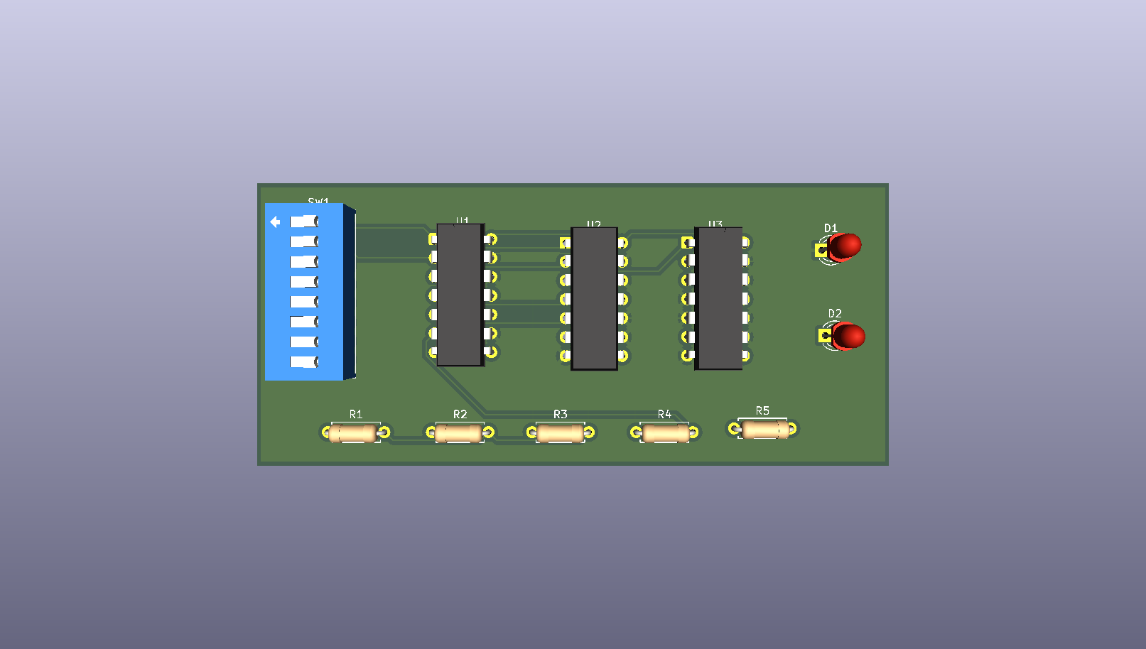
Status: Schematic, PCB layout, and manufacturing exports are included. The image above is a KiCad render, not a photograph of an assembled board. Physical fabrication and testing are not documented in this repository; exported Gerbers do not by themselves establish manufacturing readiness.
A full adder adds three one-bit inputs: A, B, and carry-in (Cin). It produces a sum bit and carry-out (Cout).
| A | B | Cin | Sum | Cout |
|---|---|---|---|---|
| 0 | 0 | 0 | 0 | 0 |
| 0 | 0 | 1 | 1 | 0 |
| 0 | 1 | 0 | 1 | 0 |
| 0 | 1 | 1 | 0 | 1 |
| 1 | 0 | 0 | 1 | 0 |
| 1 | 0 | 1 | 0 | 1 |
| 1 | 1 | 0 | 0 | 1 |
| 1 | 1 | 1 | 1 | 1 |
This is the expected logic behavior, not a record of measured hardware results.
| Folder | Contents |
|---|---|
| hardware | Editable KiCad project, schematic, and routed PCB |
| docs | Schematic PDF exports and 3D board preview |
| manufacturing | Front/back copper, solder mask, silkscreen, board outline, plated/non-plated drill files, and Gerber job file |
Open the schematic PDF for a quick look without KiCad. A second supplied schematic export is preserved as schematic-alternate-export.pdf.
| Reference | Component | Quantity |
|---|---|---|
| U1 | 74LS86 XOR logic IC | 1 |
| U2 | 74LS08 AND logic IC | 1 |
| U3 | 74LS32 OR logic IC | 1 |
| SW1 | 8-position DIP switch | 1 |
| R1–R3 | 10 kΩ resistors | 3 |
| R4–R5 | 330 Ω resistors | 2 |
| D1–D2 | LEDs | 2 |
The schematic uses +5 V and GND power nets. The supplied Gerber job describes a two-layer, 1.6 mm board with an approximately 85.05 × 38.05 mm outline. These are exported design settings, not measured board dimensions.
hardware/Full_Adder_PCB.kicad_pro in KiCad. The supplied exports identify KiCad 10.0.6.Before ordering a board, run ERC and DRC, review any unconnected nets, and confirm power connections, IC supply decoupling, unused gate inputs, switch input levels, and LED drive against the component datasheets. No passing ERC/DRC report is included here.
The source files and manufacturing exports retain the original design contents. Upload-added filename suffixes were removed so the KiCad project files share a base name and the Gerber job references resolve correctly. Temporary KiCad lock files and machine-local .kicad_prl settings are excluded.
Designed by Adhyayan Tiwari.
| Qty | Value | Footprint | References |
|---|---|---|---|
| 3 | 10k | Resistor_THT:R_Axial_DIN0207_L6.3mm_D2.5mm_P7.62mm_Horizontal | R1, R2, R3 |
| 2 | 330 | Resistor_THT:R_Axial_DIN0207_L6.3mm_D2.5mm_P7.62mm_Horizontal | R4, R5 |
| 2 | LED | LED_THT:LED_D3.0mm | D1, D2 |
| 1 | 74LS08 | Package_DIP:DIP-14_W7.62mm | U2 |
| 1 | 74LS32 | Package_DIP:DIP-14_W7.62mm | U3 |
| 1 | 74LS86 | Package_DIP:DIP-14_W7.62mm | U1 |
| 1 | SW_DIP_x08 | Button_Switch_THT:SW_DIP_SPSTx08_Slide_9.78x22.5mm_W7.62mm_P2.54mm | SW1 |
It measures 85 × 38 mm and has 2 copper layers, 1.6 mm thick.
11 parts, built around the 74LS32SC and 74LS86. The full list of its parts is on this page, with links to each part's symbol and footprint where PCBKit's library has them.
From the adhyayan15/full-adder-pcb repository on GitHub, at the commit this page was made from: the board is hardware/Full_Adder_PCB.kicad_pcb and its schematic hardware/Full_Adder_PCB.kicad_sch. PCBKit opens the board in the browser, with nothing to install.
Its repository states no licence, so its author keeps all rights: ask adhyayan15 before reusing the design.
The-Invent0r/8-bit-Computer-PCB
These are the KiCAD files for my 8-Bit Computer.

hkzlab/CGA_Redux
The Color Graphics Adapter Redux board is a more or less faithful clone of the original IBM CGA, based on the original schematics

profdc9/ISACard
A ISA card for PC/XT/AT that has SD storage and SPI/I2C interfaces using a ATMEGA328P

btb/LanguageCard
An Apple II Language Card. Based on a design by iz8dwf


fortinsylvain/MyCpu
Home brew CPU Hardware with 1-bit ALU implementation using 74LSxx, a micro-code and assembler coded in C#.

clemarfolly/Microdigital-TK2000
Reprodução da PCB do TK-2000 da Microdigital, clone do Micro-Professor MPF-II
