

2 layers100 × 100 mm

 acwright/6502-VCS3
6502-VCS 8-Bit Retro Computer Project
Flash Cart is an open-source printed circuit board by acwright, from the acwright/6502-VCS repository on GitHub, published under the CERN-OHL-P-2.0 licence. It is a 2-layer board of 81.8 × 57.6 mm with 25 parts on 70 nets, routed with 837 tracks and 222 vias.
It is built around the 74HC32D, 74HC138 and 74HC139D, with the 74HC1G04GW and 74HC273D among its other parts. Its parts include 9 capacitors, 8 ICs and 1 connector. It belongs with the retro computing and games boards of this library.


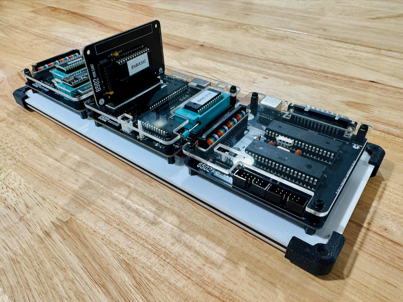
An AC6502 retro-style 8-bit computer based on the 65C02 microprocessor.
📖 Guide: AC6502 Documentation — the user's and programmer's guide for the whole family. See VCS's page in the family appendix.
Building one? Every part you need, with supplier numbers and known issues, is in BOM.md.
EXP0–EXP3 and HRDBThe AC6502 ecosystem is a family of open-source, 65C02-based computers sharing a common architecture, memory map, and BIOS. Each computer in the family is purpose-built for a different use case but runs the same software and firmware.
The VCS is a cartridge-based retro gaming console. It features a real 65C02 CPU, swappable ROM cartridges, VGA video output via Pico9918, SID audio via ARMSID, and support for PS/2 keyboards, matrix keyboards, and Atari 2600-compatible joysticks.
All AC6502 computers share:
| Project | Description |
|---|---|
| 6502-ACE | All-in-one Computer Experience — A single board computer |
| 6502-COB | Computer On a Backplane — Modular desktop computer with expandable card slots |
| 6502-DEV | Development Environment Vehicle — Emulation-based dev system |
| 6502-KIM | Keypad Input Monitor - KIM-1 inspired minimal computer |
| 6502-VCS | Video Computer System — Cartridge-based retro gaming console (YOU ARE HERE) |
| Project | Description |
|---|---|
| 6502-BIOS | The shared BIOS (kernel, monitor, BASIC) for all AC6502 computers |
| 6502-EMULATOR | Emulator for the whole family — desktop app, browser build, and a command line for scripted runs |
| 6502-PRG | Template project for writing assembly language programs |
| 6502-CRT | Template project for writing assembly language cartridges |
| 6502-ASM | Assembly language example programs and demos |
| 6502-BAS | BASIC program listings |
| 6502-WOZMON | Wozmon as a standalone ROM |
| 6502-NOP | An all-NOP ROM, for probing a board during bring-up |
| 6502-DOCS | The documentation site — the guide, the printable reference cards, branding and label artwork |
| cffs | Builds CompactFlash disk images for the BIOS filesystem |
| bastok | Tokenizes BASIC listings into .prg images, and back |
| bin2woz | Converts a binary into a Wozmon serial upload |
This repository contains KiCad 7.0+ PCB designs for the boards that make up the VCS system.
Hardware/Main Board/
The core board containing the 65C02 CPU, 32KB SRAM, 32KB EEPROM, clock, and reset circuitry. Runs at 1 MHz and provides the bus connection for the Input and Output boards.
Hardware/Input Board/
Unified input board supporting a matrix keyboard, PS/2 keyboard, and Atari 2600-compatible joysticks. Uses a 65C22 VIA and an ATmega1284 microcontroller as the keyboard encoder controller.
The joysticks share the VIA ports with the keyboard encoder rather than having connectors of their own: they come in on the J1 PORT B and J2 PORT A box headers, with JOY(1) reading PORT B and JOY(2) reading PORT A. See Joystick Interface for the wiring options and the bitmask the BIOS returns.
Hardware/Output Board/
Combined VGA video output (via Raspberry Pi Pico running Pico9918) and SID audio output (via ARMSID). Provides TMS9918A-compatible graphics modes at 640×480 VGA and 3-voice SID synthesis.
Hardware/ROM Cart/
Swappable ROM cartridge for the VCS system. Comes in two versions:
Hardware/Flash Cart/
Banked flash cartridge, and the successor to the fixed 16K ROM Cart. One all-SMD board covers 128KB to 1MB, depending on which parts are populated, and the flash is programmed in circuit through the card edge, either by the Flash Helper (an Arduino Mega 2560 shield with one connector on it) or by the 6502 itself.
$C000–$DFFF is a switchable 8K window, selected by a write-only bank register at $E000–$FFFF.$E000–$FFFF is fixed to the last 8K of the primary flash, so the vectors and the bank-switching code can
never be mapped out.See DESIGN.md for the memory map, the logic, the programming sequences and the build variants.
Hardware/Flash Helper/
The programmer for the Flash Cart: an Arduino Mega 2560 R3 shield with a cartridge slot on it, and nothing else. It pretends to be the 65C02 on the far side of the card edge, so a cart is programmed in circuit with no chip ever removed — which matters, because the flash is a soldered-down TSOP part.
A0–A15, D0–D7, RWB, PHI2, RESB, IRQB, NMIB,
VCC and GND.EXP0 and EXP1 are deliberately not connected. Cartridges tie them to GND to disable the
system ROM, so driving them would be a short.6502-flash, a Node CLI. See DESIGN.md.As a card tester. Every card in the AC6502 family — the COB
cards, the KIM Keypad Card and both VCS carts — carries the same
6502 Card Edge fingers and drops into this socket. IRQB and NMIB are wired for that reason rather
than for programming: the GPIO, LCD, Serial and Serial Card Pro cards all assert IRQB, and a tester
that could not see it would miss most of what they do. That firmware is a separate build and does not
exist yet.
Make the newest revision of a board, and check its label first. The table below gives each board's newest revision. A newer revision fixes what was found on the older ones. Every revision, old and new, is in REVISIONS.md, with what changed in each.
Each revision carries one of three labels:
BOM.md has the parts for every revision, and its known issues.
| Board | Newest revision | Label | Why |
|---|---|---|---|
| Flash Cart | 1.0 | Untested | Made, and not tested yet. |
| Flash Helper | 1.0 | Untested | Made, and not tested yet. |
| Input Board | 1.1 | Proven design | Silkscreen text only. |
| Main Board | 1.1 | Proven design | 10k pull-ups, small part moves and tracks rerouted. The jumpers are gone, and HRDB is wired as it is on the tested Rev 1.0 with them fitted. |
| Output Board | 1.1 | Proven design | Silkscreen text, and the VDD header removed. |
| ROM Cart | 1.0a or 1.0b | Tested | Rev 1.0a takes an AT28C256 EEPROM; Rev 1.0b takes an AT27C256 EPROM. |
This repository contains PlatformIO-based firmware for the Input Board.
Firmware/IB Controller/
Firmware for the ATmega1284 on the Input Board. Provides:
See Firmware/IB Controller/README.md for setup and usage instructions.
CAD/
3D-printable enclosure parts and laser-cut top panels for the VCS system.
Board images are in CAD/Images/<Board>/Rev X/: Front.png and Back.png on white, and Front Transparent.png and Back Transparent.png with no background. Every image is a 3D render at the same size, with the black solder mask and white silkscreen the boards are made with. Bare-board photos may differ, because the renders show parts fitted.
Top panels are versioned by board revision, like Hardware/: CAD/Tops/<Board>/Rev X/. Each revision has its own complete folder, even when two revisions share the same files. Bases/ holds the parts for a whole computer, not for one board, so it isn't versioned.
The plate mounting drawing (SVG) shows where the Output Board, the Main Board and the Input Board mount on the base plate, with every hole's position and the hardware the build needs. The plate is a stack of three 3 mm acrylic layers.
Production/
REVISIONS.md lists every board revision: whether it was made, its JLCPCB order, the commit it was made from, and what fits it.
JLCPCB-ready Gerber files and BOM/CPL for PCB fabrication and assembly.
Schematics/
PDF schematics for each board.
Five lines of the 6502 bus are shared by every board on it: RESB, IRQB, NMIB, RDY and BE. A board may pull one of these lines low, and nothing drives one high. Each line is held high by one 10kΩ pull-up resistor to VCC, on the board with the CPU: the ACE Board, the KIM Board, the VCS Main Board, the COB CPU Card or CPU Card Pro, or the DEV Board. No other board has one. Two pull-ups on the same line would sit in parallel and lower its resistance, so a card that adds its own pull-up changes the machine for every other board. The VIAs and PIAs in the BOMs, the W65C22N and W65C21N, have open-drain interrupt outputs for this reason. A W65C22S drives IRQB high as well as low, so it can't share the line without a diode.
The same holds where a board has its own reset circuit. A reset switch, its timer and the transistor that pulls RESB low can be on any board, such as the COB Backplane Pro or the Clock Card, but the RESB pull-up is only ever on the board with the CPU. Each of those boards draws its pull-ups together, in one group on its schematic.
SOB is a CPU pin that isn't on the bus. It is tied to VCC, directly or through a 10kΩ resistor.
A few chips have a pull-up of their own inside the chip, such as an ATmega's reset pin. Where such a pin is wired to RESB, its pull-up of 30–60kΩ sits in parallel with the 10kΩ one. That's harmless, because whatever pulls RESB low can sink the extra current many times over.
A revision that doesn't follow this yet says so in its known issues in BOM.md, with what to fit or remove.
EXP0–EXP3 and HRDBEXP stands for "extra pin". Four pins of the 6502 bus are left for a builder's own use: pin 4 is EXP1, pin 6 is EXP0, pin 19 is EXP3 and pin 21 is EXP2.
Pins 4 and 6 have a second job. A cartridge ties both of them to GND. That pulls HRDB ("High ROM disable bar", active low) low on the board with the ROM, which takes $C000–$FFFF away from the ROM so that the cartridge answers there instead. So in a build that uses cartridges, pins 4 and 6 are reserved for HRDB, and nothing else may drive them. They are free as EXP1 and EXP0 only in a build that never uses cartridges. EXP2 and EXP3 are always free.
How the boards treat pins 4 and 6:
HRDB input, and their silk says HRDB. The VCS Main Board joins them the same way from Rev 1.1.HRDB only through jumpers: fit two shunts on J2, or bridge JP1 and JP2, in a COB that takes cartridges. It is the only board with these jumpers, because the COB is the experimenter's build. The VCS Main Board Rev 1.0 had them too (J5, or JP3 and JP4); fit them, because the VCS always takes cartridges.EXP1 and EXP0, as its silk does, and a note on its schematic says what they carry.Some boards have solder jumpers, and pin headers that take a shunt. The tables below give every one: what it's for, how the board is shipped, and what to do with it. The Needed column marks the ones that matter:
Where a header needs a shunt, the board's BOM lists it.
Input Board
| Rev | Jumper | What it's for | As shipped | What to do | Needed |
|---|---|---|---|---|---|
| 1.0, 1.1 | J6 | I/O window: one shunt picks the 1 KB window the board answers in. | No shunt. | Fit the shunt beside $9400: IO 6, where the BIOS looks for the Input Board. | To run |
| 1.0, 1.1 | JP1 | Bridged across D1, the diode in the VIA's interrupt line. | Bridged. | Leave it. The VIA's interrupt output only pulls low, so D1 isn't needed. Cut JP1 only for a part that drives its interrupt high as well as low. |
Main Board
| Rev | Jumper | What it's for | As shipped | What to do | Needed |
|---|---|---|---|---|---|
| 1.0 | J5, JP3, JP4 | HRDB EN: joins the bus's EXP1 and EXP0 to the ROM's High ROM disable. | Open, no shunts. | Fit two shunts on J5, or bridge JP3 and JP4: without them a cartridge can't take $C000–$FFFF, and the VCS always takes cartridges. Rev 1.1 wires them. | For cartridges |
| 1.0 | J8 | EXP EN: shunts here join CPU signals (VPB, MLB, SOB, PHI1O, PHI2O) to the bus's extra pins. | No shunts. | Leave it empty: the VCS takes cartridges, which ground EXP0 and EXP1. Rev 1.1 has no J8. | |
| 1.0 | JP1, J2 | ROM WE: joins the ROM's /WE to the write strobe, so a program can write the EEPROM in circuit. | Open, no shunt. | Leave it open: R1 holds /WE high. Rev 1.1 ties /WE to VCC. | |
| 1.0 | JP2, J1 | Power: JP2 is across J1 (PWR_SW), the header for a power switch. | Open. | Bridge JP2, or wire a switch to J1. Until one is done the board has no power. Rev 1.1 has neither. | To run |
| 1.0 | JP5, J7 | Original 6502: grounds pin 1, which is VSS on an NMOS 6502 and VPB on a 65C02. | Open, no shunt. | Leave both open for a 65C02. Rev 1.1 has neither. | |
| 1.0 | JP6, J6 | Clock: JP6 is across J6 (CLOCK_ENBL_SW), the header for a switch that stops the clock. | Open. | Bridge JP6, or wire a switch to J6. Until one is done there is no clock on PHI2. Rev 1.1 has neither. | To run |
Output Board
| Rev | Jumper | What it's for | As shipped | What to do | Needed |
|---|---|---|---|---|---|
| 1.0, 1.1 | J6 | Interrupt: one shunt sends the board's interrupt to IRQB or NMIB. | No shunt. | Fit the shunt on IRQB, which the BIOS expects. With no shunt the interrupt reaches neither. | For interrupts |
| 1.0, 1.1 | J7 | I/O windows: two shunts pick the windows for the sound chip and the video chip. | No shunts. | Fit one shunt beside $9800 (IO 7) for the sound chip and one beside $9C00 (IO 8) for the video chip, where the BIOS looks for them. | To run |
| 1.0 | JP1 | Bridged across D1, the diode in the pico9918's interrupt line. | Bridged. | Cut JP1. The pico9918 drives its interrupt high as well as low, and only D1 stops it holding IRQB high against the Input Board, as on the VGA Card 1.0. Rev 1.1 ships it open. | For interrupts |
| 1.0, 1.1 | JP3, JP2 | JP3 feeds PHI2 to an enable of U3, a 74HC138, so the board is selected only while PHI2 is high. JP2 would tie that enable high instead. | JP3 bridged, JP2 open. | Leave them. | |
| 1.1 | JP1 | Bridged across D1, the diode in the pico9918's interrupt line. | Open. | Leave it open: the pico9918 drives its interrupt high as well as low, and D1 lets it only pull IRQB low. Never bridge it. |
Some boards have small headers, such as RESET SW, CLOCK ENBL SW, POWER LED and VCC, that a standard build leaves empty. They are for a machine built into a full enclosure, which AC6502 doesn't offer today. In such a build, the parts a person handles are mounted on the case and wired to the board through these headers: the power jack, the switches, the LEDs and the keyboard. The matching parts on the board are then left off. For example, an ACE Board can sit inside a case with its power jack, power switch and key switches left off, and a Keyboard Helper as its keyboard.
To build a board for a case:
The connector follows the kind of build. A single-board machine, the ACE Board or the KIM Board, uses plain 2.54 mm pin headers, which are simpler and cheaper. A board in a multi-board machine, every COB board and the separate boards of the VCS, the DEV and the KIM, uses JST XH, the family's standard for these headers.
The table lists every off-board header on each board's newest revision, read from the board's PCB file.
| Board | Rev | Header | Label | Connector | What it's for | Leave off |
|---|---|---|---|---|---|---|
| Main Board | 1.1 | J4 | RESET SW | JST XH, 2 pins | A reset button on the case. The header is wired across SW1, the board's own reset button. | SW1, if the case covers it. Both buttons reset the machine if it stays. |
Libraries/
Shared KiCad symbol and footprint libraries used across all AC6502 hardware projects, with their 3D models in Models/. A part is named for what it is and its shape, such as RJ45 Jack LED or CR2032 Holder, never for a manufacturer's part number, so a replacement part with the same footprint fits without renaming anything. The part numbers to buy are in BOM.md. Every AC6502 repository carries the same copy of each part.
Every part for every board, by revision, is in BOM.md, with supplier numbers, known issues, build notes and files to upload to Digi-Key and Mouser. What changed in each revision, and what is known about each one, is in REVISIONS.md.
Hardware designs are released under the CERN Open Hardware Licence Version 2 – Permissive.
Firmware is released under the MIT License.
| Qty | Value | Footprint | References |
|---|---|---|---|
| 8 | 100nF | Capacitor_SMD:C_0603_1608Metric | C1, C2, C3, C4, C5, C6, C7, C8 |
| 2 | 74HC32 | Package_SO:SOIC-14_3.9x8.7mm_P1.27mm | U6, U7 |
| 2 | MountingHole | MountingHole:MountingHole_3.2mm_M3 | H1, H2 |
| 2 | MountingHole | MountingHole:MountingHole_2.2mm_M2 | H3, H4 |
| 2 | SST39SF040 | Package_SO:TSOP-I-32_11.8x8mm_P0.5mm | U1, U2 |
| 1 | 10uF | Capacitor_SMD:C_0805_2012Metric | C9 |
| 1 | 6502 Card Edge | 6502 Parts:6502 Card Edge | J1 |
| 1 | 74HC138 | Package_SO:SOIC-16_3.9x9.9mm_P1.27mm | U4 |
| 1 | 74HC139 | Package_SO:SOIC-16_3.9x9.9mm_P1.27mm | U5 |
| 1 | 74HC1G04 | Package_TO_SOT_SMD:SOT-23-5 | U8 |
| 1 | 74HC273 | Package_SO:SOIC-20W_7.5x12.8mm_P1.27mm | U3 |
| 1 | LOGO | A.C. Wright Logo:A.C. Wright Logo 5mm | G*** |
| 1 | LOGO | 6502 Logos:6502 Flash Cart Logo 5mm | G*** |
The 24 most common of 25 parts.
It measures 81.8 × 57.6 mm and has 2 copper layers, 1.6 mm thick.
25 parts, built around the 74HC32D, 74HC138, 74HC139D and 74HC1G04GW. The full list of its parts is on this page, with links to each part's symbol and footprint where PCBKit's library has them.
From the acwright/6502-VCS repository on GitHub, at the commit this page was made from: the board is Hardware/Flash Cart/Rev 1.0/Flash Cart.kicad_pcb and its schematic Hardware/Flash Cart/Rev 1.0/Flash Cart.kicad_sch. PCBKit opens the board in the browser, with nothing to install.
Its repository publishes it under the CERN-OHL-P-2.0 licence: you may reuse it on that licence's terms (keep the author's notice, and for a copyleft licence share your changes alike).


Cptscorcher/Excallibur-64
A reimagining of the seminal Excalibur 64 Computer


KITTY-6502/hardware
the KITTY is a 65c02 homebrew kit microcomputer designed around text mode graphics and cartridge media. It is fully open source, and uses exclusively in-production parts.


ifilot/p2000t-ram-expansion-board
RAM expansion board for the P2000T