

2 layers335 × 250 mm

 acwright/6502-ACE12
6502-ACE 8-Bit Retro Computer Project
ACE Board is an open-source printed circuit board by acwright, from the acwright/6502-ACE repository on GitHub, published under the CERN-OHL-P-2.0 licence. It is a 2-layer board of 335 × 250 mm with 204 parts on 214 nets, routed with 4,074 tracks and 1,256 vias.
It is built around the ATMEGA1284-PU, 74HC00D and 74HC138, with the 74HC573, 74HC163D and 74HC30S among its other parts. Its parts include 45 switches, 35 resistors, 30 capacitors, 20 ICs and 12 connectors. It belongs with the retro computing and games boards and the AVR (ATmega, ATtiny) boards of this library.


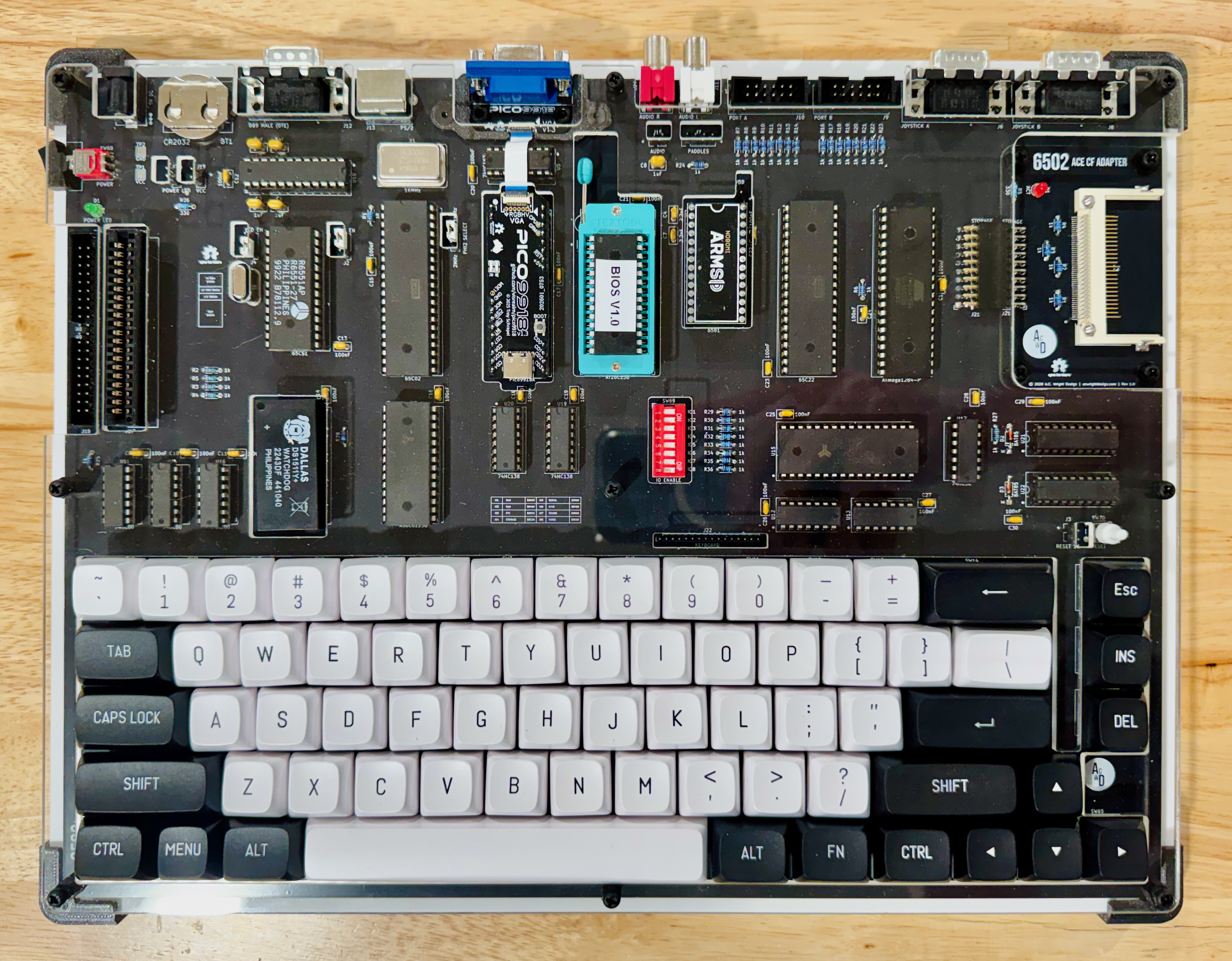
An AC6502 retro-style 8-bit computer based on the 65C02 microprocessor.
📖 Guide: AC6502 Documentation — the user's and programmer's guide for the whole family. Start with Your ACE, the tour of this board.
Building one? Every part you need, with supplier numbers and known issues, is in BOM.md.
EXP0–EXP3 and HRDBThe AC6502 ecosystem is a family of open-source, 65C02-based computers sharing a common architecture, memory map, and BIOS. Each computer in the family is purpose-built for a different use case but runs the same software and firmware.
The ACE (All-in-one Computer Experience) is a complete, self-contained 65C02 computer on a single PCB. It integrates everything found across the COB's modular cards — CPU, memory, video, audio, storage, serial, GPIO, RTC, and keyboard controller — onto one board, delivering the full experience without a backplane or expansion cards.
All AC6502 computers share:
| Project | Description |
|---|---|
| 6502-ACE | All-in-one Computer Experience — A single board computer (YOU ARE HERE) |
| 6502-COB | Computer On a Backplane — Modular desktop computer with expandable card slots |
| 6502-DEV | Development Environment Vehicle — Emulation-based dev system |
| 6502-KIM | Keypad Input Monitor - KIM-1 inspired minimal computer |
| 6502-VCS | Video Computer System — Cartridge-based retro gaming console |
| Project | Description |
|---|---|
| 6502-BIOS | The shared BIOS (kernel, monitor, BASIC) for all AC6502 computers |
| 6502-PICOVDP | Firmware for the ACE's video card, on a PICO9918 PRO v2.0 |
| 6502-EMULATOR | Emulator for the whole family — desktop app, browser build, and a command line for scripted runs |
| 6502-PRG | Template project for writing assembly language programs |
| 6502-CRT | Template project for writing assembly language cartridges |
| 6502-ASM | Assembly language example programs and demos |
| 6502-BAS | BASIC program listings |
| 6502-WOZMON | Wozmon as a standalone ROM |
| 6502-NOP | An all-NOP ROM, for probing a board during bring-up |
| 6502-DOCS | The documentation site — the guide, the printable reference cards, branding and label artwork |
| cffs | Builds CompactFlash disk images for the BIOS filesystem |
| bastok | Tokenizes BASIC listings into .prg images, and back |
| bin2woz | Converts a binary into a Wozmon serial upload |
This repository contains KiCad 7.0+ PCB designs for the ACE board.
Hardware/ACE Board/
The single integrated board hosting the W65C02S CPU and all peripherals. Provides:
Pico9918ARTS, DTR and DSR
always reach the cable; the CTS EN and DCD EN jumpers (J2 and J4 on Rev 1.0, J1 and J3 on Rev 1.1) pick ground or the cable for
those two inputs — both default to groundJ6 and J8 on Rev 1.0, J5 and J7 on Rev 1.1), read as JOY(2) and JOY(1) respectivelyThe serial handshake jumpers. CTS EN and DCD EN (J2 and J4 on Rev 1.0, J1 and J3 on Rev 1.1) both default to ground, and
that is how the boards were built. Ground means the line is permanently asserted, so the ACIA can
always send and always receive. Moved to the cable, they do real work — measured on a real R6551 in
2026: CTS high stops the transmitter dead and DCD high stops the receiver, losing the byte that
arrives. A board jumpered to the cable and plugged into something that does not assert those lines
shows no banner and no echo at all, and looks broken when it is not.
D5); Rev 1.0 has noneCards on CART and BUS. IRQB, NMIB and RESB are shared by several devices on the board and by
anything plugged into CART and BUS (J17 and J18). A card may only pull
those lines low, open-drain, and must never drive them high: a device that drives a shared line high holds it
there against every other device that pulls it low. A video card built around a pico9918 has the same /INT
problem as U3, and needs the same diode on the card.
BSY with a loop counted in CPU cycles, about 851 ms at 1 MHz. Every card tested is found, but a slower card could be missed. A probe that waits a fixed time is planned for the next BIOS 2.x update (6502-BIOS TODO.md, item 1).Hardware/ACE CF Adapter/
A CompactFlash adapter board that connects to the Storage header on the ACE Board. Provides:
J21 for STORAGE and J3 for the CF socket. See the revision historyHardware/ACE RAM Patch/
A patch board for Rev 1.0 of the ACE Board that corrects the extended RAM (banked SRAM) decoding, with the same logic as Rev 1.1. U12 and U13 come off the ACE, chips and sockets, and the patch is soldered underneath in their place. Provides:
LOADL and LOADH go high only on a write to the bank register, $83FF or $87FF, while PHI2 is high. Rev 1.0 pulsed both latches whenever the bus was idle, and the first patch (Rev 1.0) fixed that but still loaded a latch on any write to $8300–$83FE and $80FF–$82FF (and the same in the $8400 window)Tests/check-schematics.mjs, and on 2026-11-03 an ACE Board Rev 1.0 with the patch fitted passed node Tests/check-ram.mjs --expect FF with every card in place: HW_PRESENT read $FF after each of 10 restarts, each latch loaded only on its own address, and every bank of both windows held its own patterns, with 0 failures in 3 runs. The same board had 0 failures in 3 runs without the video card and the CF Adapter, reading $77. Without the patch, a Rev 1.0 reads $FD, because the BIOS doesn't find the $8400 window. See Checking the banked RAMMake the newest revision of a board, and check its label first. The table below gives each board's newest revision. A newer revision fixes what was found on the older ones. Every revision, old and new, is in REVISIONS.md, with what changed in each.
Each revision carries one of three labels:
BOM.md has the parts for every revision, and its known issues.
| Board | Newest revision | Label | Why |
|---|---|---|---|
| ACE Board | 1.1 | Untested | A new bank-latch decode (its logic is proven on the ACE RAM Patch 1.1), 1 MHz only, and a 1N5819 in the power path. On the first build, measure VCC at full load: it must stay above 4.5 V. |
| ACE CF Adapter | 1.1 | Proven design | Annotation only. The new LCSC socket fits the same footprint, but no board has been built with it yet. |
| ACE RAM Patch | 1.1 | Tested | Built and tested on an ACE Board Rev 1.0, 2026-11-03. |
This repository contains PlatformIO-based firmware for the ACE board. The video card's firmware is 6502-PICOVDP, and the ROM is 6502-BIOS.
The ACE runs a PICO9918 PRO v2.0 (RP2354A) with 6502-PICOVDP, and BIOS 2.x. RP2040 PICO9918 boards (v1.x) can't run 6502-PICOVDP.
MDE1 pin: solder one 0.1″ header pin into the PRO's MDE1 pad.picotool save -a stock.bin. To restore it later, picotool load -v -x stock.bin. The backup has been made on a PRO; the restore is picotool's ordinary load and hasn't been tried.picovdp-v1.0.0.uf2 from the v1.0.0 release (SHA-256 0b74cd9875cbffc46de7ec48a9bb6e0d4a76a3e796d2563615e17e6bed94afd5). Hold BOOT, connect USB-C, and run picotool load -v -x -f picovdp-v1.0.0.uf2. The release build has no USB of its own, so every update needs BOOT again. The card can be flashed in the ACE's socket with the ACE switched off.v2.0.2.AC6502 BIOS v2.0, BASIC v2.0 30718 BYTES FREE and RAM RTC CF SER VIA SID VDP, at power-on and after the reset button (SW70 on Rev 1.0, SW17 on Rev 1.1). If VDP is missing from that line, the card isn't running 6502-PICOVDP.MDE1 pin from BASIC: POKE 39939,4:POKE 39939,142:PRINT PEEK(39939):POKE 39939,0:POKE 39939,142 prints 172.On Rev 1.0, fit the /INT diode first (see Building a Rev 1.0).
Firmware/AB Controller/
Firmware for the ATmega1284 keyboard controller on the ACE board. Provides:
RESB low on PC7, open-drain, holding the CPU in reset for ~250 ms at power-on, and debounces the reset button on PC0NMIB low from the DS1511Y SQW input, open-drain; compiled out unless ENABLE_SQW is defined. The ENABLE_SQW build compiles, but hasn't been run on hardwareSee Firmware/AB Controller/README.md for setup and usage instructions.
CAD/
3D-printable enclosure bases and laser-cut top panels for the ACE system.
Board images are in CAD/Images/<Board>/Rev X/: Front.png and Back.png on white, and Front Transparent.png and Back Transparent.png with no background. Every image is a 3D render at the same size, with the black solder mask and white silkscreen the boards are made with. Bare-board photos may differ, because the renders show parts fitted.
Top panels and jigs are versioned by board revision, like Hardware/: CAD/Tops/<Board>/Rev X/, CAD/Jigs/<Board>/Rev X/. Each revision has its own complete folder, even when two revisions share the same files. Bases/ holds the parts for a whole computer, not for one board, so it isn't versioned.
The plate mounting drawing (SVG) shows where the ACE Board and the ACE CF Adapter mount on the base plate, with every hole's position and the hardware the build needs. The plate is a stack of three 3 mm acrylic layers.
Production/
REVISIONS.md lists every board revision: whether it was made, its JLCPCB order, the commit it was made from, and what fits it.
JLCPCB-ready Gerber files and BOM/CPL for PCB fabrication and assembly.
Schematics/
PDF schematics for the ACE board.
Five lines of the 6502 bus are shared by every board on it: RESB, IRQB, NMIB, RDY and BE. A board may pull one of these lines low, and nothing drives one high. Each line is held high by one 10kΩ pull-up resistor to VCC, on the board with the CPU: the ACE Board, the KIM Board, the VCS Main Board, the COB CPU Card or CPU Card Pro, or the DEV Board. No other board has one. Two pull-ups on the same line would sit in parallel and lower its resistance, so a card that adds its own pull-up changes the machine for every other board. The VIAs and PIAs in the BOMs, the W65C22N and W65C21N, have open-drain interrupt outputs for this reason. A W65C22S drives IRQB high as well as low, so it can't share the line without a diode.
The same holds where a board has its own reset circuit. A reset switch, its timer and the transistor that pulls RESB low can be on any board, such as the COB Backplane Pro or the Clock Card, but the RESB pull-up is only ever on the board with the CPU. Each of those boards draws its pull-ups together, in one group on its schematic.
SOB is a CPU pin that isn't on the bus. It is tied to VCC, directly or through a 10kΩ resistor.
A few chips have a pull-up of their own inside the chip, such as an ATmega's reset pin. Where such a pin is wired to RESB, its pull-up of 30–60kΩ sits in parallel with the 10kΩ one. That's harmless, because whatever pulls RESB low can sink the extra current many times over.
A revision that doesn't follow this yet says so in its known issues in BOM.md, with what to fit or remove.
EXP0–EXP3 and HRDBEXP stands for "extra pin". Four pins of the 6502 bus are left for a builder's own use: pin 4 is EXP1, pin 6 is EXP0, pin 19 is EXP3 and pin 21 is EXP2.
Pins 4 and 6 have a second job. A cartridge ties both of them to GND. That pulls HRDB ("High ROM disable bar", active low) low on the board with the ROM, which takes $C000–$FFFF away from the ROM so that the cartridge answers there instead. So in a build that uses cartridges, pins 4 and 6 are reserved for HRDB, and nothing else may drive them. They are free as EXP1 and EXP0 only in a build that never uses cartridges. EXP2 and EXP3 are always free.
How the boards treat pins 4 and 6:
HRDB input, and their silk says HRDB. The VCS Main Board joins them the same way from Rev 1.1.HRDB only through jumpers: fit two shunts on J2, or bridge JP1 and JP2, in a COB that takes cartridges. It is the only board with these jumpers, because the COB is the experimenter's build. The VCS Main Board Rev 1.0 had them too (J5, or JP3 and JP4); fit them, because the VCS always takes cartridges.EXP1 and EXP0, as its silk does, and a note on its schematic says what they carry.Some boards have solder jumpers, and pin headers that take a shunt. The tables below give every one: what it's for, how the board is shipped, and what to do with it. The Needed column marks the ones that matter:
Where a header needs a shunt, the board's BOM lists it.
ACE Board
| Rev | Jumper | What it's for | As shipped | What to do | Needed |
|---|---|---|---|---|---|
| 1.0 | J1 | PHI2 SELECT: the CPU clock, 1 MHz (pins 1 and 2) or 2 MHz (pins 2 and 3). | No shunt. | Fit the shunt on pins 1 and 2, 1 MHz: at 2 MHz the sound chip, whose clock is always 1 MHz, answers only every other cycle. With no shunt the CPU has no clock. | To run |
| 1.0 | J2 | CTS: where the ACIA's CTS comes from. | No shunt. | Fit the shunt on pins 1 and 2, ground, as the boards are built. On pins 2 and 3 it takes CTS from the cable, and a cable that doesn't assert it stops the transmitter. With no shunt the input floats, and serial may not work. | For serial |
| 1.0 | J4 | DCD: where the ACIA's DCD comes from. | No shunt. | Fit the shunt on pins 1 and 2, ground, as the boards are built. On pins 2 and 3 it takes DCD from the cable, and a cable that doesn't assert it stops the receiver. With no shunt the input floats, and serial may not work. | For serial |
| 1.1 | J1 | CTS: where the ACIA's CTS comes from. | No shunt. | Fit the shunt on pins 1 and 2, ground, as the boards are built. On pins 2 and 3 it takes CTS from the cable, and a cable that doesn't assert it stops the transmitter. With no shunt the input floats, and serial may not work. | For serial |
| 1.1 | J3 | DCD: where the ACIA's DCD comes from. | No shunt. | Fit the shunt on pins 1 and 2, ground, as the boards are built. On pins 2 and 3 it takes DCD from the cable, and a cable that doesn't assert it stops the receiver. With no shunt the input floats, and serial may not work. | For serial |
Some boards have small headers, such as RESET SW, CLOCK ENBL SW, POWER LED and VCC, that a standard build leaves empty. They are for a machine built into a full enclosure, which AC6502 doesn't offer today. In such a build, the parts a person handles are mounted on the case and wired to the board through these headers: the power jack, the switches, the LEDs and the keyboard. The matching parts on the board are then left off. For example, an ACE Board can sit inside a case with its power jack, power switch and key switches left off, and a Keyboard Helper as its keyboard.
To build a board for a case:
The connector follows the kind of build. A single-board machine, the ACE Board or the KIM Board, uses plain 2.54 mm pin headers, which are simpler and cheaper. A board in a multi-board machine, every COB board and the separate boards of the VCS, the DEV and the KIM, uses JST XH, the family's standard for these headers.
The table lists every off-board header on each board's newest revision, read from the board's PCB file.
| Board | Rev | Header | Label | Connector | What it's for | Leave off |
|---|---|---|---|---|---|---|
| ACE Board | 1.1 | J2 | RESET SW | Pin header, 1×2, 2.54 mm | A reset button on the case. The header is wired across SW17, the board's own reset button. | SW17, if the case covers it. Both buttons reset the machine if it stays. |
| ACE Board | 1.1 | J13 | KEYBOARD | Pin header, 1×16, 2.00 mm | The keyboard matrix: PA0–PA7 on pins 1–8 and PB0–PB7 on pins 9–16. A keyboard on the case, such as a Keyboard Helper, connects here. | The key switches, SW1–SW16 and SW18–SW68. |
| ACE Board | 1.1 | J15 | AUDIO | Pin header, 1×2, 2.54 mm | Audio to a jack or an amplifier on the case: the same signal as J10 and J14, on pin 1, with ground on pin 2. | J10 and J14, if the case has its own jack. They can stay fitted beside it. |
| ACE Board | 1.1 | J19 | VCC | Pin header, 1×2, 2.54 mm | Power from a jack and a switch on the case: 5 V on pin 1, ground on pin 2. The header is on VCC itself, past D5, the reverse-polarity diode, and SW69, the power switch. | J16, the barrel jack, and SW69, the power switch. Nothing on the board protects this header, so the case's supply must be a regulated 5 V, wired the right way around. |
| ACE Board | 1.1 | J20 | POWER LED | Pin header, 1×2, 2.54 mm | A power LED on the case: anode to pin 1 (VCC), cathode to pin 2, which runs through R25 to ground. | D2, the board's own power LED. It shares R25, so with both fitted each gets half the current. |
Docs/
ACE Board Rev 1.0 Build Notes (PDF, for printing): the work a Rev 1.0 needs beyond its bill of materials, step by step. That is the pull-up values, the ACIA, the supply capacitor, the RESB pull-up and firmware, the /INT diode's socket stack and fitting the ACE RAM Patch, followed by the meter checks and the first power-on.
Tests/check-schematics.mjs
The banked RAM's latch enables were wrong in Rev 1.0, and wrong again in a different way in the first RAM Patch, and both times the gates looked right on paper. This script checks the logic instead of reading it. It asks KiCad for each board's netlist, builds the glue logic from the gates it finds there, and drives every address, as a read and as a write, with PHI2 high and low and with a cartridge in and out. That is 524,288 bus states per board. For each one it compares every chip select, read and write strobe, and bank latch enable against the memory map, and checks that exactly one chip drives the data bus on a read and exactly one takes a write. A net that nothing drives counts as a failure, so a missing wire fails too.
It checks two boards: Rev 1.1, and Rev 1.0 with the ACE RAM Patch Rev 1.1 fitted. The patch's headers name the sockets they plug into (74HC00 (U12)), and the script pulls those chips and joins each header pin to its socket's net. For Rev 1.1 it also checks that the CPU, VIA, ACIA and SID all run from U5's 1 MHz output, that the video card's /INT reaches IRQB only through a diode, and that RESB has a pull-up.
Run it after any change to either schematic:
node Tests/check-schematics.mjsIt needs Node.js and KiCad's kicad-cli, which it finds on the PATH, at the macOS default location, or through a KICAD_CLI environment variable. It takes about 15 seconds, prints ok or FAIL for each check with example bus states for any failure, and exits non-zero on a failure.
Tests/check-ram.mjs
check-schematics.mjs checks the logic as it is drawn. This script checks a built board, including its chips, its solder joints and, on a Rev 1.0, its ACE RAM Patch. It talks to the machine over the serial port. It restarts the machine ten times and reads HW_PRESENT after each boot, then loads Tests/check-ram.asm over XMODEM and runs it three times. The program does three things:
$83FF and $87FF, isn't tested.The boot probe alone can't confirm the decode fix. The BIOS tests only banks 0 and 1, so a machine with the first RAM Patch's decode still finds its RAM.
Connect the ACE's serial port, start it at BASIC's prompt on BIOS 2.x, and run:
node Tests/check-ram.mjsWith every card fitted, add --expect FF to require that exact HW_PRESENT. Without it, only the two RAM bits have to be set. --port, --runs and --restarts change the defaults; the top of the script lists them.
It needs Node.js, cc65 and stty, so it runs on macOS and Linux. It takes about four minutes, works with or without a video card, and exits non-zero on a failure. It erases the BASIC program in memory and everything in the banked RAM.
Tests/check-ram-fault.cjs shows that the test can fail. It runs the program on the emulator with a fault added to the emulated RAM card: the first RAM Patch's decode, a stuck latch bit, or a latch that never loads. Each fault has to produce failures. The file's header has the command.
Libraries/
Shared KiCad symbol and footprint libraries used across all AC6502 hardware projects, with their 3D models in Models/. A part is named for what it is and its shape, such as RJ45 Jack LED or CR2032 Holder, never for a manufacturer's part number, so a replacement part with the same footprint fits without renaming anything. The part numbers to buy are in BOM.md. Every AC6502 repository carries the same copy of each part.
Every part for every board, by revision, is in BOM.md, with supplier numbers, known issues, build notes and files to upload to Digi-Key and Mouser. What changed in each revision, and what is known about each one, is in REVISIONS.md.
Hardware designs are released under the CERN Open Hardware Licence Version 2 – Permissive. Firmware is released under the MIT License.
| Qty | Value | Footprint | References |
|---|---|---|---|
| 34 | 1k | Resistor_THT:R_Axial_DIN0204_L3.6mm_D1.6mm_P5.08mm_Horizontal | R1, R2, R10, R11, R12, R13, R14, R16, R17, R18, R19, R20, R21, R22, R23, R24 +18 |
| 23 | 100nF | Capacitor_THT:C_Disc_D5.0mm_W2.5mm_P2.50mm | C1, C10, C11, C12, C13, C14, C15, C16, C17, C18, C19, C20, C21, C22, C23, C24 +7 |
| 9 | MountingHole | MountingHole:MountingHole_3.2mm_M3 | H1, H2, H2, H2, H2, H2, H2, H3, H4 |
| 5 | 1uF | Capacitor_THT:C_Disc_D5.0mm_W2.5mm_P2.50mm | C2, C3, C5, C6, C8 |
| 5 | 74HC00 | Package_DIP:DIP-14_W7.62mm_Socket_LongPads | U11, U12, U13, U14, U16 |
| 2 | 2.2nF | Capacitor_THT:C_Disc_D5.0mm_W2.5mm_P2.50mm | C4, C7 |
| 2 | 74HC138 | Package_DIP:DIP-16_W7.62mm_Socket_LongPads | U19, U20 |
| 2 | 74HC573 | Package_DIP:DIP-20_W7.62mm_Socket_LongPads | U21, U22 |
| 2 | ALT | 6502 Parts:SW_Cherry_MX_1.25u_PCB | SW59, SW67 |
| 2 | BAT85 | Diode_THT:D_DO-35_SOD27_P7.62mm_Horizontal | D2, D3 |
| 2 | CTRL | 6502 Parts:SW_Cherry_MX_1.25u_PCB | SW58, SW66 |
| 2 | MountingHole | MountingHole:MountingHole_2.2mm_M2 | H3, H3 |
| 2 | SHIFT | 6502 Parts:SW_Cherry_MX_2.25u_PCB | SW41, SW49 |
| 1 | ' | 6502 Parts:SW_Cherry_MX_1.00u_PCB | SW43 |
| 1 | , | 6502 Parts:SW_Cherry_MX_1.00u_PCB | SW54 |
| 1 | - | 6502 Parts:SW_Cherry_MX_1.00u_PCB | SW12 |
| 1 | . | 6502 Parts:SW_Cherry_MX_1.00u_PCB | SW55 |
| 1 | / | 6502 Parts:SW_Cherry_MX_1.00u_PCB | SW56 |
| 1 | 0 | 6502 Parts:SW_Cherry_MX_1.00u_PCB | SW11 |
| 1 | 1 | 6502 Parts:SW_Cherry_MX_1.00u_PCB | SW2 |
| 1 | 1.8432 Mhz | Crystal:Crystal_HC49-U_Vertical | Y1 |
| 1 | 16MHz | Oscillator:Oscillator_DIP-14 | X1 |
| 1 | 2 | 6502 Parts:SW_Cherry_MX_1.00u_PCB | SW3 |
| 1 | 3 | 6502 Parts:SW_Cherry_MX_1.00u_PCB | SW4 |
| 1 | 330 | Resistor_THT:R_Axial_DIN0204_L3.6mm_D1.6mm_P5.08mm_Horizontal | R26 |
| 1 | 4 | 6502 Parts:SW_Cherry_MX_1.00u_PCB | SW5 |
| 1 | 5 | 6502 Parts:SW_Cherry_MX_1.00u_PCB | SW6 |
| 1 | 5V DC | Connector_BarrelJack:BarrelJack_Horizontal | J16 |
| 1 | 6 | 6502 Parts:SW_Cherry_MX_1.00u_PCB | SW7 |
| 1 | 6581 | Package_DIP:DIP-28_W15.24mm_Socket_LongPads | U9 |
| 1 | 65C02 | Package_DIP:DIP-40_W15.24mm_Socket_LongPads | U1 |
| 1 | 65C22 | Package_DIP:DIP-40_W15.24mm_Socket_LongPads | U2 |
| 1 | 65C51 | Package_DIP:DIP-28_W15.24mm_Socket_LongPads | U4 |
| 1 | 7 | 6502 Parts:SW_Cherry_MX_1.00u_PCB | SW8 |
| 1 | 74HC163 | Package_DIP:DIP-16_W7.62mm_Socket_LongPads | U5 |
| 1 | 74HC30 | Package_DIP:DIP-14_W7.62mm_Socket_LongPads | U17 |
| 1 | 8 | 6502 Parts:SW_Cherry_MX_1.00u_PCB | SW9 |
| 1 | 9 | 6502 Parts:SW_Cherry_MX_1.00u_PCB | SW10 |
| 1 | ; | 6502 Parts:SW_Cherry_MX_1.00u_PCB | SW42 |
| 1 | = | 6502 Parts:SW_Cherry_MX_1.00u_PCB | SW13 |
| 1 | A | 6502 Parts:SW_Cherry_MX_1.00u_PCB | SW32 |
| 1 | AS6C4008 | Package_DIP:DIP-32_W15.24mm_Socket_LongPads | U15 |
| 1 | AS6C62256 | Package_DIP:DIP-28_W15.24mm_Socket_LongPads | U7 |
| 1 | AT28C256 | Socket:DIP_Socket-28_W11.9mm_W12.7mm_W15.24mm_W17.78mm_W18.5mm_3M_228-1277-00-0602J | U8 |
| 1 | ATmega1284-P | Package_DIP:DIP-40_W15.24mm_Socket_LongPads | U6 |
| 1 | AUDIO | Connector_PinHeader_2.54mm:PinHeader_1x02_P2.54mm_Vertical | J15 |
| 1 | AUDIO L | 6502 Parts:RCA Jack White | J11 |
| 1 | AUDIO R | 6502 Parts:RCA Jack White | J14 |
| 1 | B | 6502 Parts:SW_Cherry_MX_1.00u_PCB | SW51 |
| 1 | BACKSPACE | 6502 Parts:SW_Cherry_MX_2.00u_PCB | SW14 |
| 1 | BUS | 6502 Parts:6502 Bus Connector | J18 |
| 1 | C | 6502 Parts:SW_Cherry_MX_1.00u_PCB | SW48 |
| 1 | CAPS LOCK | 6502 Parts:SW_Cherry_MX_1.75u_PCB | SW31 |
| 1 | CART | 6502 Parts:6502 Card Slot | J17 |
| 1 | CR2032 | 6502 Parts:CR2032 Holder Numbered | BT1 |
| 1 | CTS EN | Connector_PinHeader_2.54mm:PinHeader_1x03_P2.54mm_Vertical | J2 |
| 1 | D | 6502 Parts:SW_Cherry_MX_1.00u_PCB | SW34 |
| 1 | DB9 MALE (DTE) | Connector_Dsub:DSUB-9_Pins_Horizontal_P2.77x2.84mm_EdgePinOffset7.70mm_Housed_MountingHolesOffset9.12mm | J12 |
| 1 | DCD EN | Connector_PinHeader_2.54mm:PinHeader_1x03_P2.54mm_Vertical | J4 |
| 1 | DELETE | 6502 Parts:SW_Cherry_MX_1.00u_PCB | SW45 |
| 1 | DOWN ARROW | 6502 Parts:SW_Cherry_MX_1.00u_PCB | SW64 |
| 1 | DS1511Y | Package_DIP:DIP-28_W15.24mm_Socket_LongPads | U18 |
| 1 | E | 6502 Parts:SW_Cherry_MX_1.00u_PCB | SW19 |
| 1 | ENTER | 6502 Parts:SW_Cherry_MX_2.25u_PCB | SW44 |
| 1 | ESCAPE | 6502 Parts:SW_Cherry_MX_1.00u_PCB | SW15 |
| 1 | F | 6502 Parts:SW_Cherry_MX_1.00u_PCB | SW35 |
| 1 | FN | 6502 Parts:SW_Cherry_MX_1.25u_PCB | SW62 |
| 1 | G | 6502 Parts:SW_Cherry_MX_1.00u_PCB | SW36 |
| 1 | GND | TestPoint:TestPoint_Pad_2.5x2.5mm | TP2 |
| 1 | H | 6502 Parts:SW_Cherry_MX_1.00u_PCB | SW37 |
| 1 | I | 6502 Parts:SW_Cherry_MX_1.00u_PCB | SW24 |
| 1 | INSERT | 6502 Parts:SW_Cherry_MX_1.00u_PCB | SW30 |
| 1 | IO ENABLE | Button_Switch_THT:SW_DIP_SPSTx08_Slide_9.78x22.5mm_W7.62mm_P2.54mm | SW69 |
| 1 | J | 6502 Parts:SW_Cherry_MX_1.00u_PCB | SW38 |
| 1 | JOYSTICK A | Connector_Dsub:DSUB-9_Pins_Horizontal_P2.77x2.84mm_EdgePinOffset7.70mm_Housed_MountingHolesOffset9.12mm | J6 |
| 1 | JOYSTICK B | Connector_Dsub:DSUB-9_Pins_Horizontal_P2.77x2.84mm_EdgePinOffset7.70mm_Housed_MountingHolesOffset9.12mm | J8 |
| 1 | K | 6502 Parts:SW_Cherry_MX_1.00u_PCB | SW39 |
| 1 | KEYBOARD | Connector_PinHeader_2.00mm:PinHeader_1x16_P2.00mm_Vertical | J22 |
| 1 | L | 6502 Parts:SW_Cherry_MX_1.00u_PCB | SW40 |
| 1 | LEFT ARROW | 6502 Parts:SW_Cherry_MX_1.00u_PCB | SW63 |
The 159 most common of 204 parts.


nailed-barnacle/Cisc-8-ttl-processor
A cut-down version of the 8080 processor using HCTTL and including a discrete ALU and instruction decoder


stonedDiscord/Automatenplatinen
Reverse engineerte Hardware aus deutschen Spielautomaten.


It measures 335 × 250 mm and has 2 copper layers, 1.6 mm thick.
204 parts, built around the ATMEGA1284-PU, 74HC00D, 74HC138 and 74HC573. The full list of its parts is on this page, with links to each part's symbol and footprint where PCBKit's library has them.
From the acwright/6502-ACE repository on GitHub, at the commit this page was made from: the board is Hardware/ACE Board/Rev 1.0/ACE Board.kicad_pcb and its schematic Hardware/ACE Board/Rev 1.0/ACE Board.kicad_sch. PCBKit opens the board in the browser, with nothing to install.
Its repository publishes it under the CERN-OHL-P-2.0 licence: you may reuse it on that licence's terms (keep the author's notice, and for a copyleft licence share your changes alike).