2 layers84 × 98 mm

 a3l6/Badge
Dirt cheap badge for Hack Canada
Badge is an open-source printed circuit board by a3l6, from the a3l6/Badge repository on GitHub. It is a 2-layer board of 77 × 86.5 mm with 54 parts on 82 nets, routed with 659 tracks and 50 vias.
It is built around the RP2040, AP2112K-3.3 and MBR0530, with the SI1308EDL among its other parts. Its parts include 26 capacitors, 12 resistors, 4 diodes, 3 connectors and 2 ICs. It belongs with the lEDs and displays boards and the RP2040 boards of this library.


This was the first serious attempt at the Hack Canada badge before the design was later simplified into the battery-free NFC badges of v3 and v4.
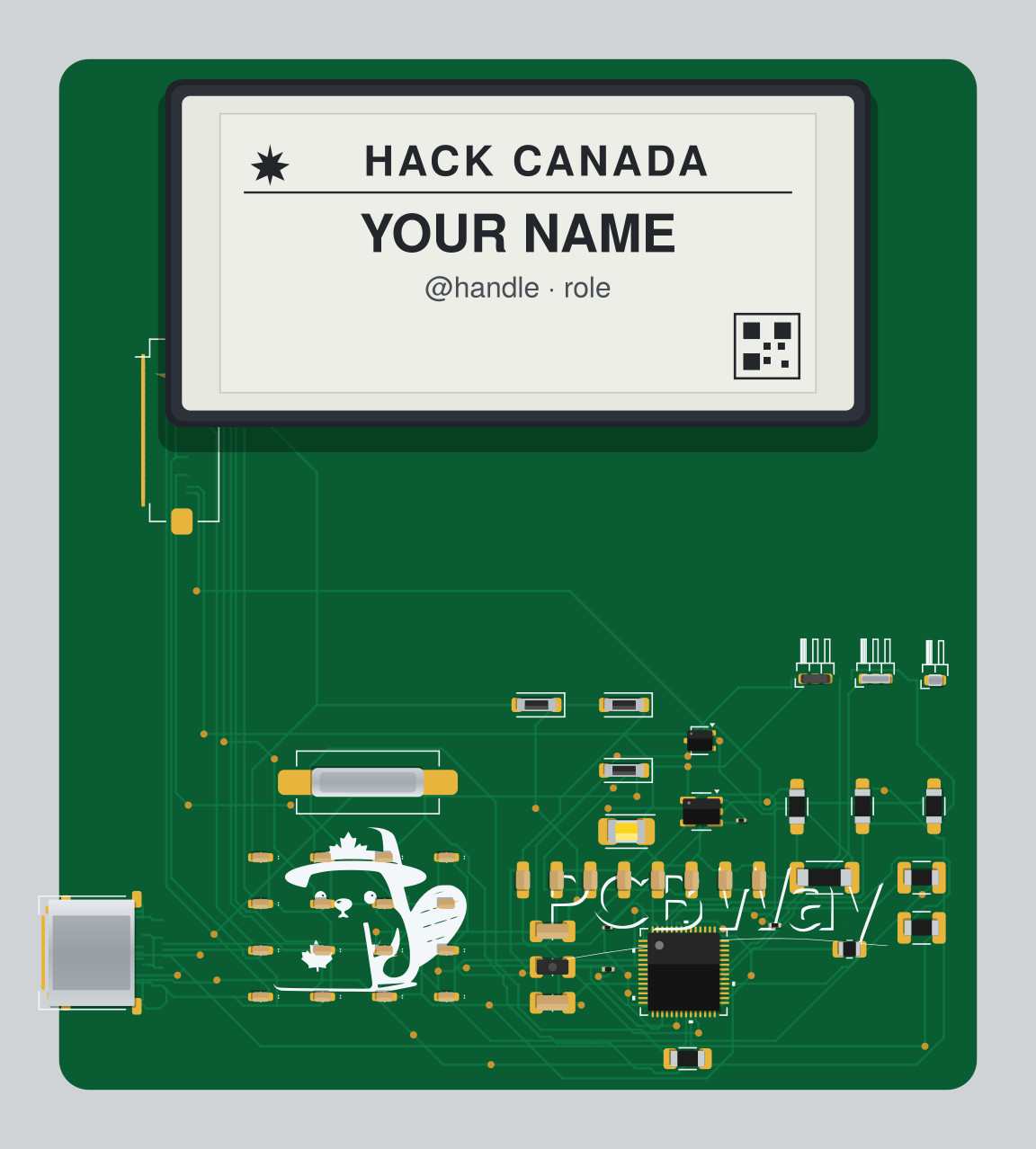
The main render shows all 51 components placed at their real board positions with the 2.13" e-paper panel mounted on top. Renders are generated from this version's Gerber files (
pcb/prod/gerber/); colours and the on-screen layout are illustrative.
Where the later revisions stripped everything down to a passive NFC tag, v2 aimed high: a programmable badge with a screen you could actually put graphics and text on. It's essentially a tiny RP2040 development board in badge form, with an e-paper panel, USB-C for power and programming, and external flash for firmware and assets.
USB-C ──► RP2040 ──► SPI ──► 2.13" e-paper display (GDEY0213F51)
            │
            ├──► QSPI ──► W25Q32 flash (firmware + images)
            ├──► 12 MHz crystal
            ├──► BOOT + RESET buttons, SWD header
            └──► status LED
Plug it in over USB-C, flash firmware to the RP2040 (BOOTSEL/UF2 or SWD), and drive the e-paper display to show a name, schedule, or artwork. The display holds its image with no power, which suits a badge that spends most of its life idle.
| Function | Part |
|---|---|
| Microcontroller | RP2040 |
| Display | GDEY0213F51 — 2.13" e-paper / E-Ink (SEEKINK panel) |
| Flash | W25Q32JVSSIQ — 32 Mbit (4 MB) SPI/QSPI |
| Clock | 12 MHz crystal (FC4SDCBMF12.0-T1) |
| Power / data | USB Type-C |
| Indicator | VLMC3100-GS08 LED |
| Protection | LESD5D5.0CT1G TVS/ESD diodes |
| Controls | BOOT + RESET buttons, SWD debug header |
| Spec | Value |
|---|---|
| Dimensions | 77.05 × 86.55 mm |
| Layers | 2 |
| Thickness | 1.6 mm |
| Designed in | KiCad 8 |
| Front | Back |
|---|---|
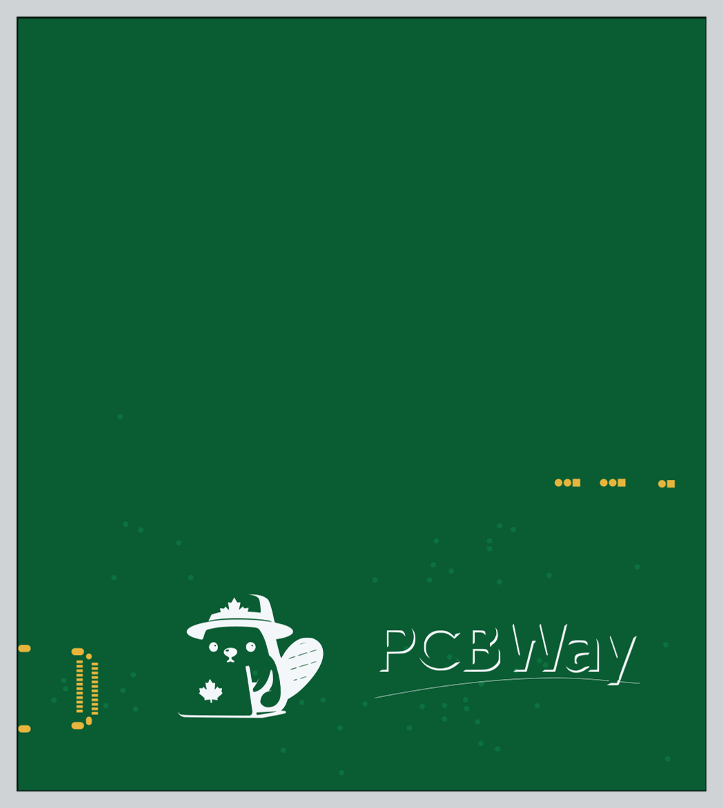 | 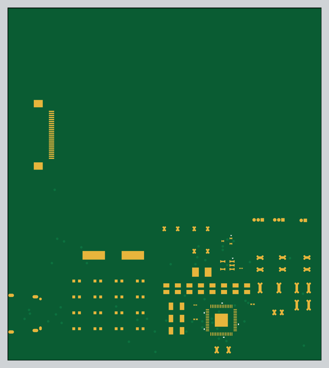 |
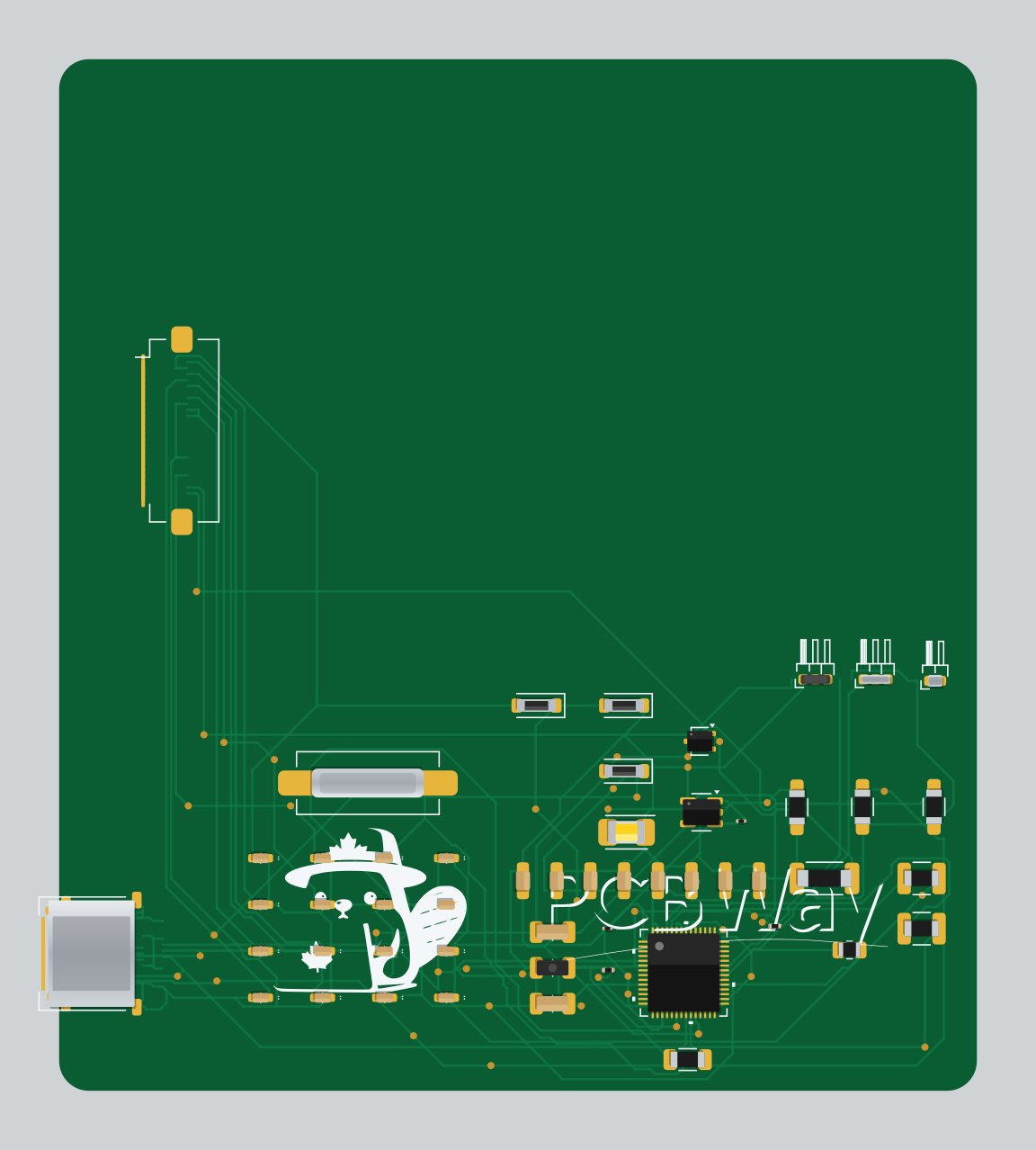
The e-paper panel (shown mounted in the main image at the top) connects over the FPC ribbon connector at the upper-left and sits above the board across the open top area, with the RP2040 and power circuitry tucked below it. The on-screen layout in that render is a placeholder mock-up, not artwork from the repo.
pcb/
├── badge.kicad_pcb / .kicad_sch / .kicad_pro   # main design
├── prod/gerber/                                # Gerbers, drills, gbrjob — ready to fab
├── badge-backups/                              # KiCad auto-backups
├── <component>/                                # per-part symbol/footprint/3D libraries
│   (RP2040, W25Q32, GDEY0213F51, crystal, LEDs, TVS, caps …)
└── assets/                                     # logos
GDEY0213F51.kicad_sym                           # e-paper display symbol
README.mdpcb/prod/gerber/ (or badge-gerbers-and-designs.zip) to your board house. It's a 2-layer, 1.6 mm board.pcb/badge.kicad_pro in KiCad 8 to modify the layout or schematic.v2 → v3 (pivot to a battery-free NFC badge, adopted from the open "Opentaxus" design) → v4 (streamlined 4-part NFC badge). See the v3 and v4 branches / READMEs.
No license file is included, so all rights are reserved by default. Contact @a3l6 to discuss reuse.
| Qty | Value | Footprint | References |
|---|---|---|---|
| 14 | 1uF | MAJCT168BB7105KTEA01:MAJx16 | C1, C2, C10, C11, C14, C15, C17, C18, C19, C20, C21, C22, C23, C25 |
| 8 | 0.1uF | footprint:CAPC2012X94N | C3, C4, C5, C6, C7, C8, C9, C16 |
| 3 | MBR0530 | Diode_SMD:D_SOD-123 | D3, D4, D5 |
| 2 | 10k | Resistor_SMD:R_01005_0402Metric | R1, R7 |
| 2 | 1k | Resistor_SMD:R_0201_0603Metric | R8, R9 |
| 2 | 27 | Resistor_SMD:R_1210_3225Metric | R2, R3 |
| 2 | 27pF | MAJCT168BB7105KTEA01:MAJx16 | C12, C13 |
| 2 | 4.7uF | GMK316AB7475KLHT:CAPC3216X180N | C24, C26 |
| 2 | 5k1 | Resistor_SMD:R_1206_3216Metric | R5, R6 |
| 2 | LOGO | LOGO | G***, G*** |
| 1 | 10k | Resistor_SMD:R_0805_2012Metric | R10 |
| 1 | 12MHz | FC4SDCBMF12.0-T1:CRYSTAL_HC49SDLF_FXT | Y1 |
| 1 | 1M | Resistor_SMD:R_2010_5025Metric | R11 |
| 1 | 2.2Ω | Resistor_SMD:R_1206_3216Metric | R12 |
| 1 | 47uH 500mA | Connector_PinHeader_1.00mm:PinHeader_1x03_P1.00mm_Horizontal | L1 |
| 1 | AP2112K-3.3 | Package_TO_SOT_SMD:SOT-23-5 | U2 |
| 1 | Conn_01x02 | Connector_PinHeader_1.00mm:PinHeader_1x02_P1.00mm_Horizontal | J2 |
| 1 | Conn_01x03 | Connector_PinHeader_1.00mm:PinHeader_1x03_P1.00mm_Horizontal | J3 |
| 1 | DNP | Resistor_SMD:R_1206_3216Metric | R4 |
| 1 | PWRLED | VLMC3100-GS08:LEDM3528X185N | D2 |
| 1 | RP2040 | RP2040:IC57_RP2040 | U1 |
| 1 | SW_Push | GMK316AB7475KLHT:CAPC3216X180N | SW1 |
| 1 | Si1308EDL | Package_TO_SOT_SMD:SOT-323_SC-70 | Q1 |
| 1 | USB_C_Receptacle_USB2.0_16P | Connector_USB:USB_C_Receptacle_Amphenol_12401610E4-2A | J1 |
| 1 | ~ | Connector_FFC-FPC:Hirose_FH12-24S-0.5SH_1x24-1MP_P0.50mm_Horizontal | GDEY0213F1 |
It measures 77 × 86.5 mm and has 2 copper layers, 1.6 mm thick.
54 parts, built around the RP2040, AP2112K-3.3, MBR0530 and SI1308EDL. The full list of its parts is on this page, with links to each part's symbol and footprint where PCBKit's library has them.
From the a3l6/Badge repository on GitHub, at the commit this page was made from: the board is pcb/badge.kicad_pcb and its schematic pcb/badge.kicad_sch. PCBKit opens the board in the browser, with nothing to install.
Its repository states no licence, so its author keeps all rights: ask a3l6 before reusing the design.


scooterthedev/E-Ink-badge
This is an e-ink USB-C PCB badge that I'm building since I loved the Github one so much, and want to make my own! I decided that I wanted to follow a similar design route with the Github Badge so I went with the RP2040…

Michael-Manning/E-Paper-Climate-Logger
Firmware, PCB, and enclosure for the Weathergotchi E-Paper climate logger.