


2 layers86.8 × 42.7 mm

 XEMACS-666/TriBit-Lux
3-Bit Flash ADC
TriBitLux V2 1 is an open-source printed circuit board by XEMACS-666, from the XEMACS-666/TriBit-Lux repository on GitHub. It is a 2-layer board of 80 × 41 mm with 61 parts on 56 nets, routed with 536 tracks and 3 vias.
It is built around the 74HCT244D, LM339 and 74LS148P-E. Its parts include 35 resistors, 7 ICs, 7 diodes, 5 capacitors and 1 connector.


One light. Eight levels. Three bits.
A light-sensing experiment, told through simulations, jumper wires and PCB designs.
3-bit flash ADC concept · LDR input · 0–7 display · KiCad + EasyEDA
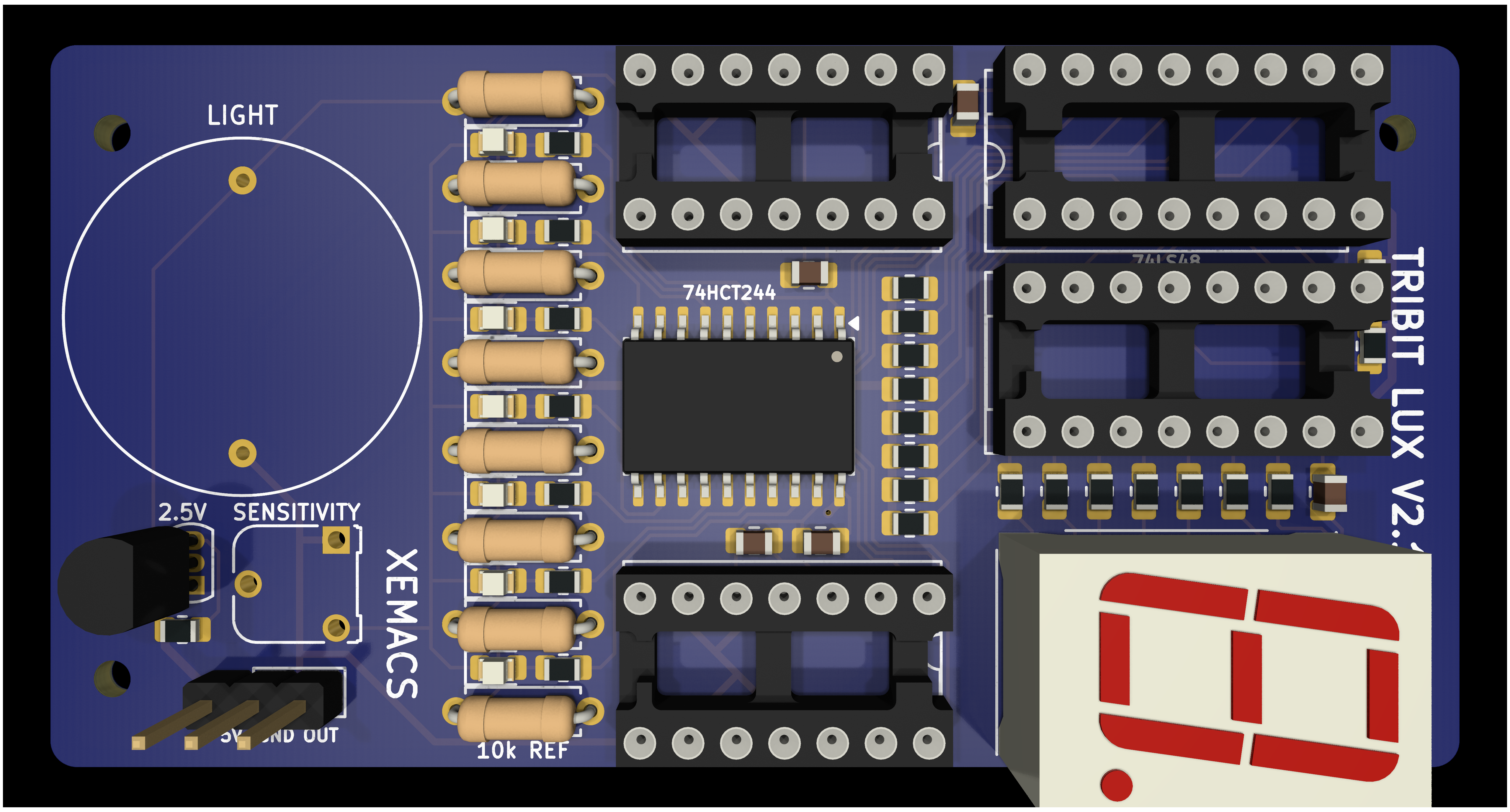
V2.1 · Compact hybrid design · 5 V input / 2.5 V reference · Not yet fabricated
Latest design · V2.1 / V2.1 design files / Version history / Interactive explorer / What's next
TriBit Lux converts an LDR's output voltage into one of eight brightness levels and shows the result on a seven-segment display. It began in TinkerCAD, moved onto breadboards, and gradually transferred the encoding and display work from an Arduino to dedicated logic ICs.
This repository presents the latest design first, followed by its earlier versions through the material saved along the way: simulations, sketches, lab photographs, schematics, interactive demonstrations and PCB exports. The breadboard wiring is part of the story—getting it into a compact board was a project in itself.
Where the project stands: V2.1 is now an 80 × 41 mm hybrid THT + SMT design with seven cumulative LEDs, a 2.5 V reference, four mounting holes and a back-side repository QR. The 30 October check reports no PCB errors, unconnected items or schematic-parity issues; 57 existing warnings remain. V2.0 stays as the unfabricated THT milestone, and V2.2 will document the fabricated result.
[blocked]
| Version | Milestone | What changed |
|---|---|---|
| V2.1 | Current hybrid design | Compact THT + SMT board, cumulative LEDs, 2.5 V reference and mounting holes. |
| V2.0 | Through-hole PCB | The breadboard connections become an unfabricated KiCad design. |
| V1.3 | LCD monitoring | An LCD adds a view of the sensor voltage. |
| V1.2 | Hardware display decoding | The 74LS48 drives the display; the Nano monitors the encoder bits. |
| V1.1 | Hardware priority encoding | The 74F148 takes over encoding; the Nano still drives the display. |
| V1.0 | First breadboard | The LDR and comparator front end move into a physical build. |
| V0.1 | LDR simulation | Light becomes the input to the simulated comparator circuit. |
| V0.0 | Potentiometer simulation | The original voltage-to-level experiment. |
V2.2 is the planned fabricated result; see what’s next.
[blocked]
80 × 41 mm · Hybrid THT + SMT · Seven cumulative LEDs · 2.5 V reference
The light-sensing circuit now fits on a compact rectangle with a regular resistor/LED column, two comparator banks, dedicated encoder and decoder ICs, and a buffer for the threshold LEDs. Four mounting holes form a symmetric 73 × 31 mm pattern. The underside carries a threshold guide and a repository QR code.
| Front · Read the layout | Back · Follow the levels |
|---|---|
 |  |
JLCPCB is planned to assemble 39 SMT parts per board; XEMACS will solder the 17 through-hole parts. The three-pin header provides 5 V input, ground and the analog sensor voltage for measurement. The nominal thresholds are spaced by 0.3125 V; the displayed level is not calibrated lux.
These are XEMACS’s existing CAD exports. They precede the 30 October silkscreen alignment; updated high-resolution renders will be supplied by XEMACS.

Click the schematic to view XEMACS’s full-resolution export.
The schematic brings together the regulated 2.5 V sensor/reference rail, the LM339 → 74LS148 → 74LS48 display path, and the 74HCT244-driven threshold LEDs. J1 provides 5 V input, ground and the analog sensor-voltage output.
Editable KiCad schematic · Current netlist · Full-resolution schematic image
Design checkpoint · 30 October 2026: PCB DRC reports zero errors, zero unconnected items and zero schematic-parity issues, with 57 existing warnings. Schematic ERC reports zero violations. The board remains unfabricated, and the next manufacturing export needs a fresh supplier DFM check. The older explorer’s V2.1 concept predates this 2.5 V implementation.
Full V2.1 gallery and files · KiCad project · Schematic · SMT BOM · SMT placement · Layout review
[blocked]
KiCad design · Through-hole components · Unfabricated
V2.0 brings the circuit into KiCad as an editable schematic and PCB. The design includes a 20 mm LDR, a potentiometer for adjusting the response, local decoupling capacitors and a regulated 3.3 V rail for the sensor divider and reference ladder.
| Sensor | Adjustment | Power and references | Construction |
|---|---|---|---|
| 20 mm LDR | Potentiometer in the divider | 5 V logic; 3.3 V sensor and ladder | Through-hole board |

Component-populated CAD preview. The LDR and potentiometer have no visible models in this render; both remain in the design and BOM.
| Read the board | Follow the routing |
|---|---|
 |  |
| Top · Silkscreen and placement | Layout · Copper and connections |

Underside of the saved PCB design. All board images here are CAD views, not fabricated hardware.
| Printed label | Circuit reference | Purpose |
|---|---|---|
| LM339-A | U1 | Upper threshold comparators plus the ground-reference comparator |
| LM339-B | U2 | Lower threshold comparators, from 0.4125 V to 1.650 V |
| 74LS148 – ENCODER | U3 | Converts active comparator inputs into three bits |
| 74LS48 – DECODER | U4 | Drives the seven-segment display |
| D198K | U5 | Displays the selected level |
| LDR / SENSITIVITY | R9 / RV1 | Light input and divider adjustment |
| 3V3 / 5V IN | U6 / J2 | Regulated reference supply and external power input |
| 0 V → 2.8875 V | R8 → R1, left to right | Nominal lower-voltage end of each 10 kΩ ladder resistor |
The ladder labels identify nominal nodes, not voltage drops across the resistors. Each resistor spans 0.4125 V ideally; the far end of R1 reaches 3.3 V. Circuit references remain in the editable design and parts lists.
The current revision includes revised capacitor footprints, a 15.5 mm lead pitch for the 20 mm LDR, a repository QR graphic, and XEMACS attribution. The custom capacitor and QR footprints are included in the project library.
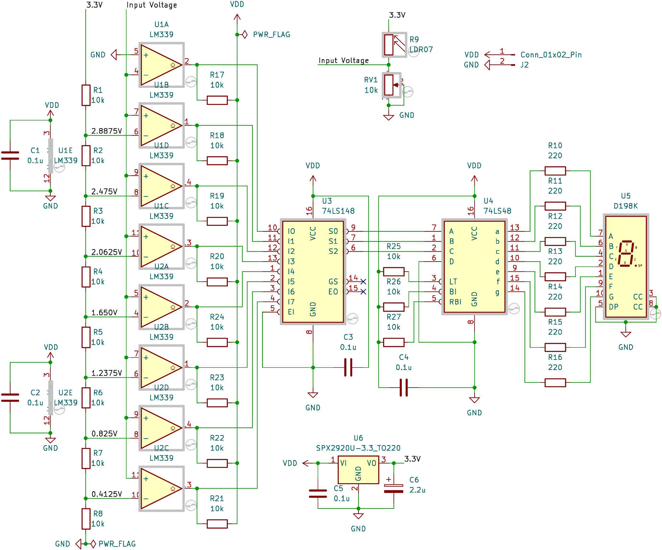
Click for the PDF, or open the scalable SVG. The older PNG export is retained as an earlier snapshot.
| Check | Result |
|---|---|
| KiCad PCB DRC | 0 reported violations; 0 unconnected items |
| Schematic ↔ PCB parity | 0 reported mismatches |
| Schematic ERC | 0 reported violations |
| BOM / placement coverage | 41 components; refreshed JLCPCB-format exports |
| Fabrication / assembly | Not performed; supplier selection and final export review remain open |
These results use the project's configured rules. Some footprint/courtyard checks are disabled; this is not a manufacturer DFM approval. See the review and remaining work for the exact limits and open items.
[blocked]
                         3.3 V reference ladder
                                  │
Light → LDR + potentiometer → LM339 comparators → Priority encoder → 74LS48 → 0–7
sensor voltage parallel decisions three bits display| Stage | What happens |
|---|---|
| 1 · Sense | Light lowers the LDR resistance. In the current divider arrangement, the sensor voltage rises as the LDR resistance falls. |
| 2 · Compare | Seven nonzero ladder references divide the nominal 0–3.3 V range into eight bands, spaced by 0.4125 V. |
| 3 · Encode | The highest-priority active LOW input determines the output. I7 through I1 receive thresholds from 0.4125 V up to 2.8875 V; I0 uses the eighth comparator with its ground reference on the opposite input. |
| 4 · Display | Encoder outputs S0, S1 and S2 connect to decoder inputs A, B and C. D is grounded, keeping the displayed range at 0–7. |
The comparator and logic ICs use 5 V. The sensor divider and reference ladder use the regulated 3.3 V rail. Earlier breadboards used a 74F148; the current V2.0 CAD source specifies a 74LS148.
About the number on the display: it is a relative brightness level, not calibrated lux. The LDR, potentiometer setting and component tolerances influence the physical transition points.
[blocked]
| Resource | Direct links |
|---|---|
| KiCad source | Project · Schematic · PCB |
| Schematic exports | PDF · Current SVG · Earlier PNG · Netlist |
| Parts lists | BOM · JLCPCB BOM |
| Placement exports | Top · Bottom · JLCPCB top |
| Manufacturing snapshot · JLCONE pass reported | Gerber ZIP |
| Custom footprints | Project library · Library table |
| Review | Checks and remaining work |
| Interactive documentation | Live explorer · Standalone HTML · GIF preview |
Open TriBitLux_V2_0.kicad_pro in KiCad to work with the schematic and PCB together. The editable files are the design sources. The JLCPCB CSVs now reflect the current component list and saved placement export. Blank supplier codes require part selection; retained codes are historical selections that still need verification. XEMACS reports that the KiCad export passed all JLCONE checks. Preserve the exact checked archive; regenerate it after any further manufacturing-layer changes. A later PCB save timestamp alone does not establish that the archive is stale.
[blocked]
Physical prototype · 16×2 I²C LCD · Parallel monitoring
The Nano gained another role: driving an LCD to make the working flow easier to follow. The hardware seven-segment path remained in place, while the Nano supplied power and sampled the LDR voltage through its own ADC.
| LCD-equipped breadboard | Another view of the build |
|---|---|
 |  |
| 5 V demonstration | 3.3 V demonstration |
|---|---|
| Open interactive 5 V view → | Open interactive 3.3 V view → |
| HTML source | HTML source |
The LCD firmware calculates its own level from the analog voltage; it does not read the encoder bits. That makes the LCD useful for observing the input, while the hardware display follows the comparator and encoder chain. These saved demonstrations belong to the V1.3 archive; the main explorer shows the updated V2.0 logic model.
Open this version: LCD sketch · Original assets
[blocked]
Physical prototype · 74LS48 decoder · Serial monitoring
Adding the 74LS48 completed the dedicated hardware display path: comparator bank → encoder → decoder → seven-segment display. The Nano supplied 5 V and received the three encoder bits so the serial console could show them for assurance.
| Overhead wiring view | Sensor and jumper connections |
|---|---|
 |  |

The powered build. The photographed display is driven by the 74LS48.
| Additional powered view | A second captured state |
|---|---|
 |  |
The last two previews link to the original HEIC photographs. Large photographs throughout this page use smaller preview copies; click them for the originals.
Open this version: Serial-monitor sketch · Original photo collection
The saved sketch includes experimental segment-driving code. In the photographed build, the 74LS48 drives the display, while the Nano observes the encoder output.
[blocked]
Physical prototype · 74F148 priority encoder · EasyEDA design exports
The 74F148 took over priority encoding from the Nano. The comparator bank now fed a dedicated logic IC, which produced the three output bits. The Nano continued to decode those bits and drive the display. This version also has an EasyEDA schematic and PCB design archive.
| Schematic beside the build | Full demonstration setup |
|---|---|
 |  |
| Schematic and wiring together | Display and reference table |
| Watching the output | Another angle of the setup |
|---|---|
 |  |
| Hardware output alongside monitoring | The complete workbench arrangement |
| Schematic | Routed PCB layout |
|---|---|
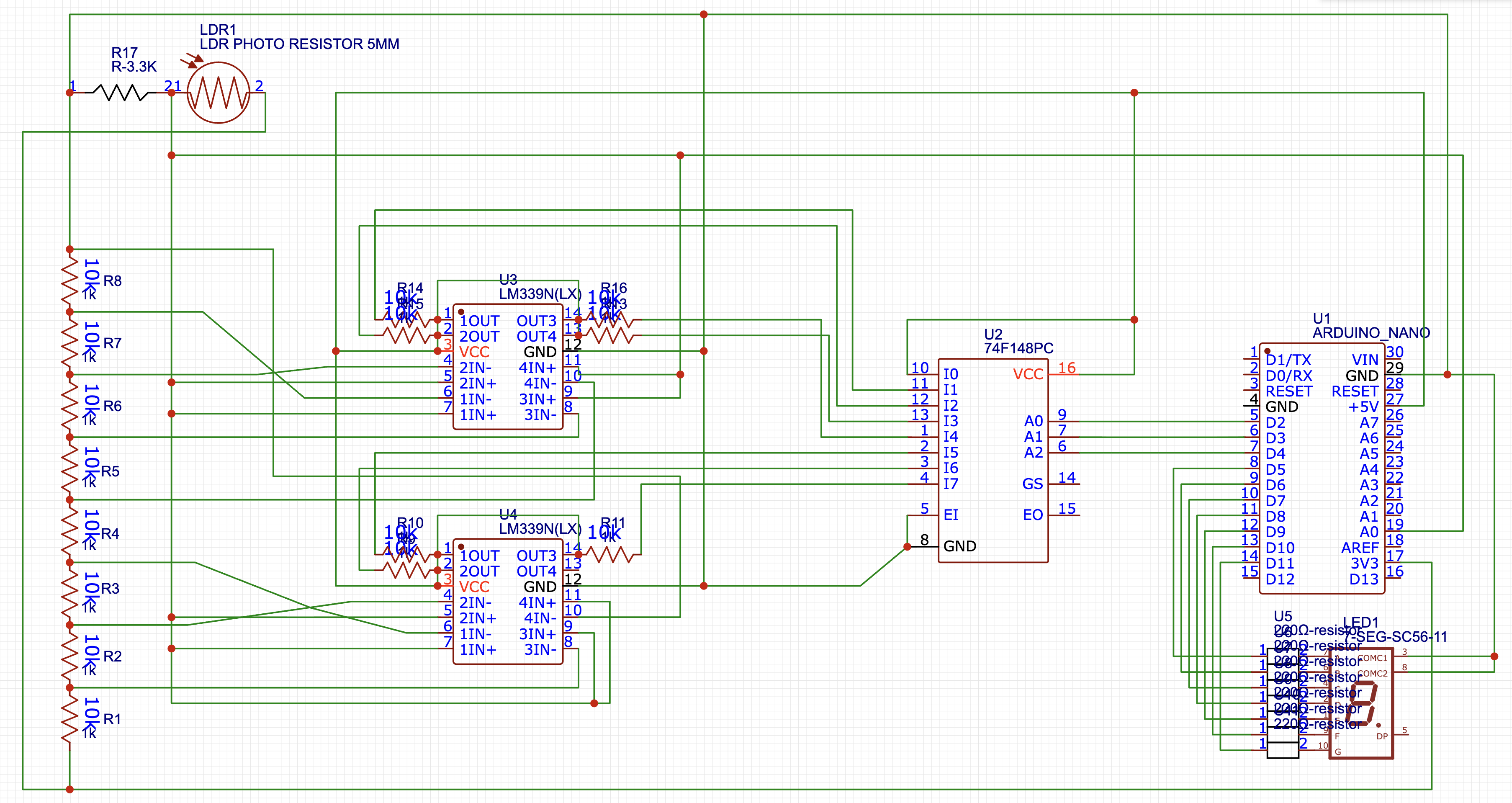 |  |

EasyEDA design render with the Nano fitted. This image documents the board design.
| Top board view · SVG | Bottom board view · SVG |
|---|---|
 |  |
Open this version: Schematic PDF · PCB PDF · Arduino sketch · BOM · Gerber archive
| Export | Top | Bottom |
|---|---|---|
| Copper | Top layer | Bottom layer |
| Silkscreen | Top silk | Bottom silk |
| Solder mask | Top mask | Bottom mask |
| Paste mask | Top paste | Bottom paste |
[blocked]
Physical prototype · Two LM339s · Arduino Nano
The LDR and comparator bank moved out of the simulator and onto a breadboard. The Nano read the comparator outputs and drove the seven-segment display. The saved recording captures the early physical build, with the jumper wiring fully on show.
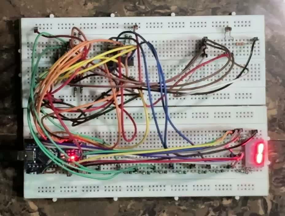
▶ Watch the breadboard recording · 24 seconds
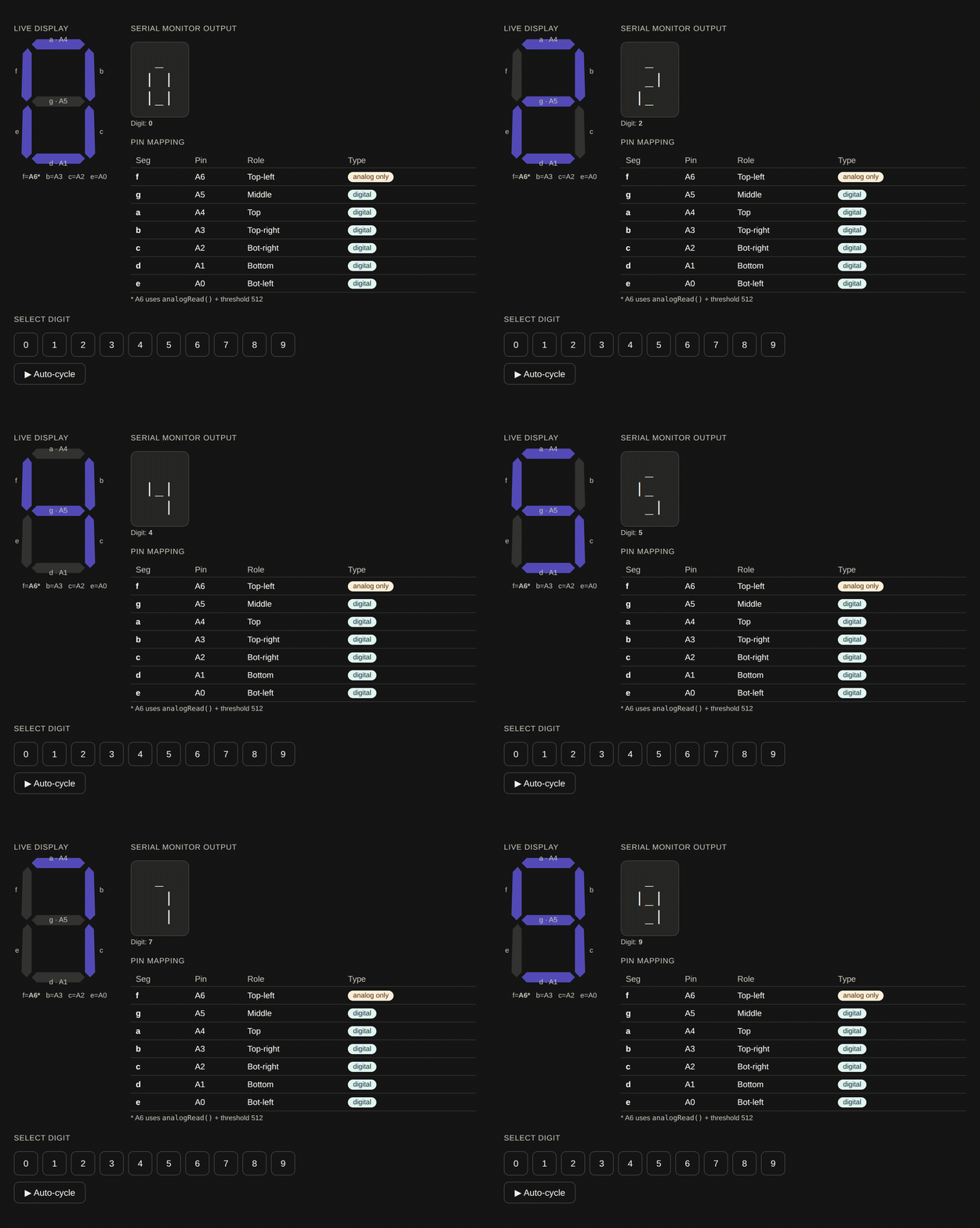
Click the animation to explore the display pin layout.
Open this version: Recording · Interactive pin guide · HTML source · Visualizer sketch
The saved visualizer sketch is a debugging aid; it is not the complete original V1.0 display firmware.
[blocked]
TinkerCAD simulation · LDR input · LM339 comparators
The potentiometer input was replaced with an LDR, and the comparator section moved to LM339 devices. Now the input responded to light. The Uno still supplied both digital stages: deciding the encoded value and converting it into segment signals.
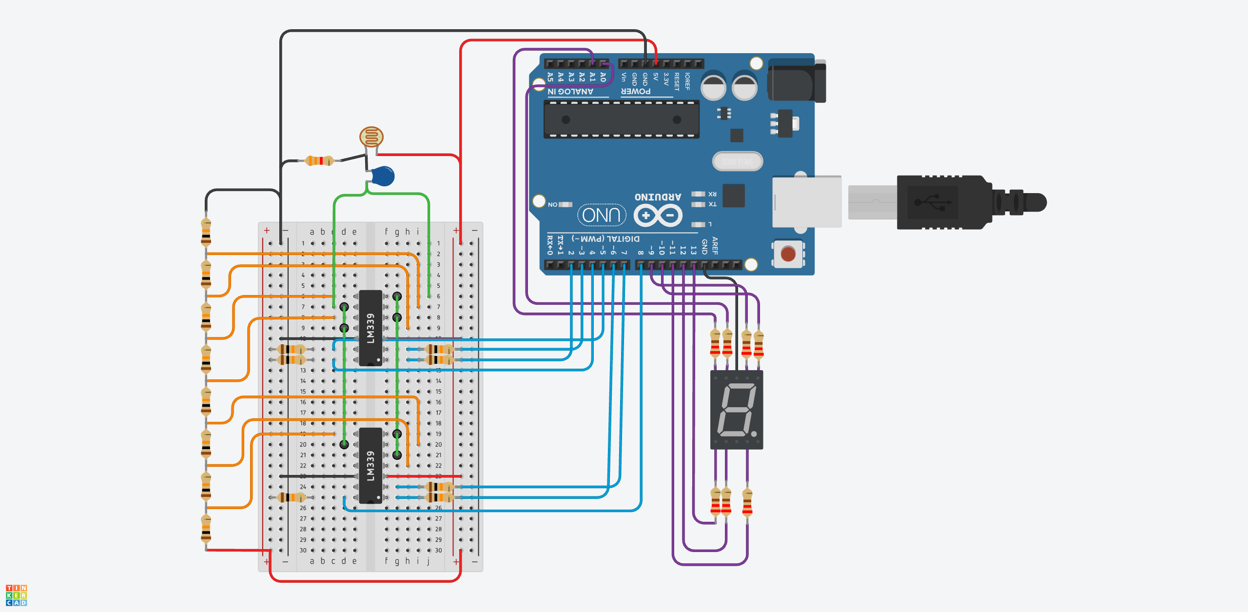
The sensor enters the picture. The display logic is still handled by the Uno.
Open this version: Simulation · Schematic PDF · Arduino sketch · BOM
[blocked]
TinkerCAD simulation · Potentiometer input · Arduino Uno
The first version used a potentiometer to stand in for the sensor voltage. Turning the knob changed the input to the comparator bank, while the Uno performed priority encoding and drove the seven-segment display. This established the basic voltage-to-level idea before adding a light-sensitive input.
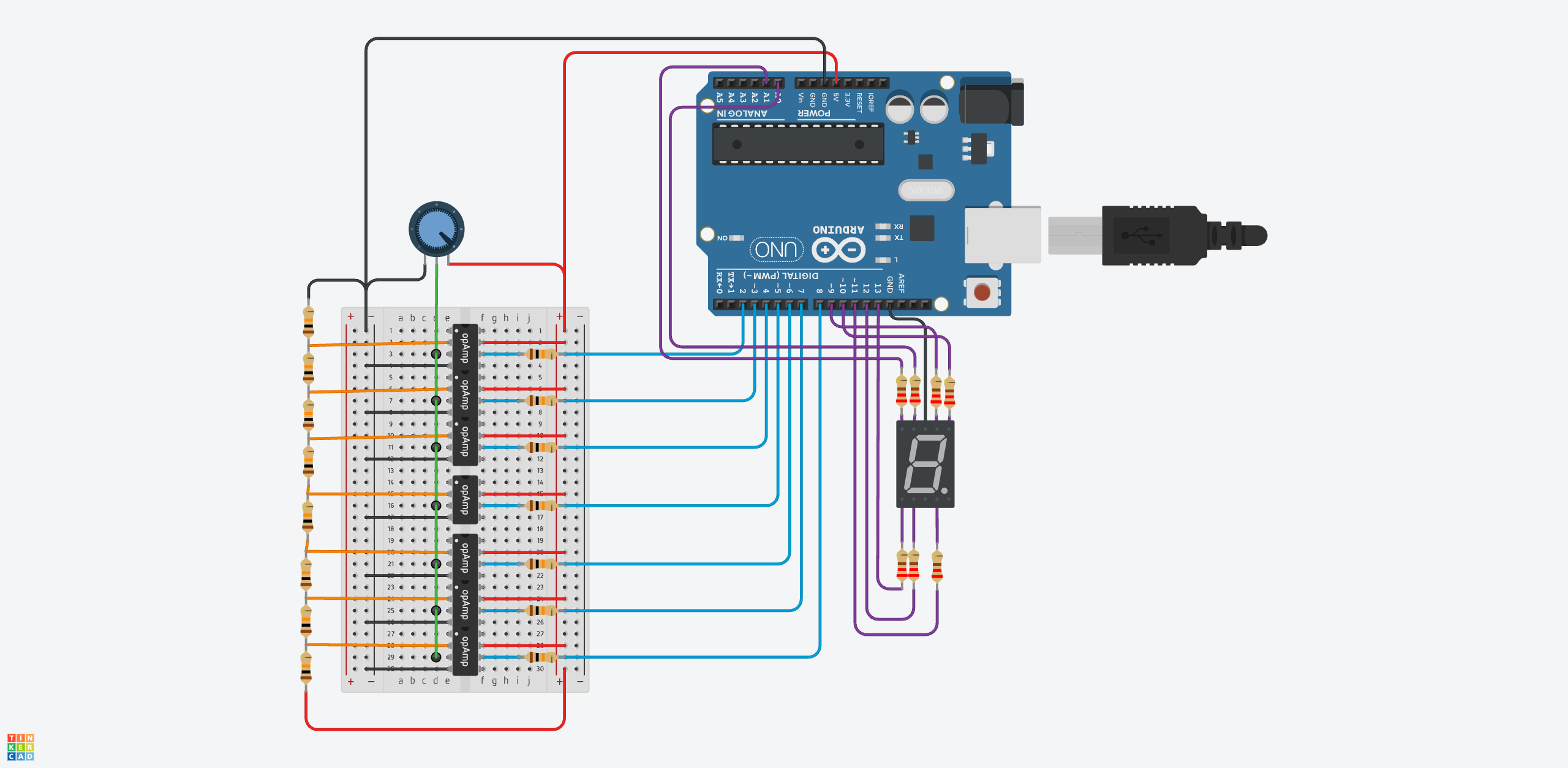
The starting point. Click the circuit image to open its TinkerCAD simulation.
Open this version: Simulation · Schematic PDF · Arduino sketch · BOM
[blocked]
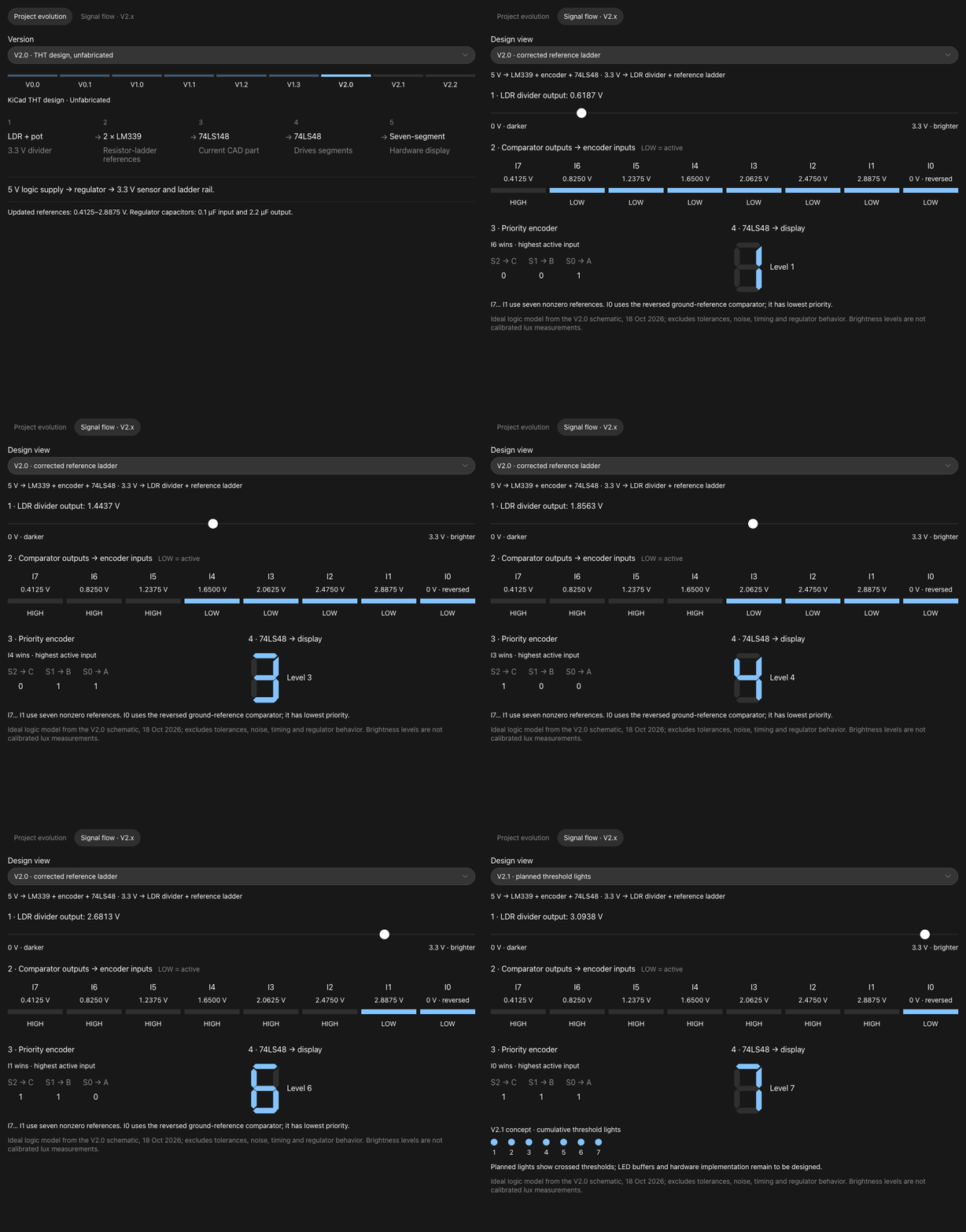
Open the interactive TriBit Lux explorer →
| Follow the evolution | Trace a signal | Preview the next revision |
|---|---|---|
| Select a version and watch the role of the Arduino change. | Move the voltage slider and follow the comparator outputs, three encoder bits and displayed digit. | Switch to the V2.1 concept to see cumulative threshold lights. |
The preview above is animated; the linked page is interactive. The explorer uses the updated V2.0 reference mapping, including the level-0 band. It models ideal logic, with real-world tolerances, noise and timing left out. Open the standalone HTML file.
[blocked]
| V2.0 · Preserve | V2.1 · Refine | V2.2 · Build |
|---|---|---|
| Keep the full THT design as an unfabricated milestone. | Review the compact 80 × 41 mm hybrid design and refresh its manufacturing exports. | Fabricate and assemble the completed design. |
| Retain its schematic, layout and development record. | Refine threshold lights, silkscreen and assembly details. | Record power-up measurements, light response and the finished assembly. |
| Current design archive | Design the acrylic enclosure around the four mounting holes and confirm the on-board QR scans reliably. | Fit the enclosure and document the physical result. |
The planned lights should make each level transition easier to see. The acrylic enclosure should make the circuit easier to display while providing secure mounting. Support components such as decoupling and protection remain electrically important whether their packages are THT or SMT.
[blocked]
TriBit-Lux/
├── README.md                    Illustrated project walkthrough
├── docs/media/                  Photo previews and video poster
├── Version_2.1/
│   ├── README.md                Hybrid board gallery, pinout and status
│   ├── TriBitLux_V2_1/          Editable KiCad project, schematic and PCB
│   ├── assets/                 XEMACS’s board renders and schematic image
│   ├── schematic/              Current netlist
│   ├── bom/                    Full and SMT-only parts lists
│   ├── cpl/                    Native and JLCPCB placement exports
│   └── review/                 Current checks and layout feedback
├── Version_2.0/                 Unfabricated through-hole milestone
├── Version_1.3/                 LCD build and demonstrations
├── Version_1.2/                 Hardware decoder and serial sketch
├── Version_1.1/                 Encoder build and EasyEDA archive
├── Version_1.0/                 First breadboard and pin visualizer
├── Version_0.1/                 LDR simulation
└── Version_0.0/                 Potentiometer simulation
Each version folder contains the records that survived that stage. Older versions may not contain a complete build package. The photographs, videos and interactive pages show the development process; the editable design files describe the circuit. KiCad temporary files and backups are excluded through .gitignore.
Built and documented by XEMACS
From a simulated input to a board designed around light.
Try the explorer · Back to the latest design · Repository
| Qty | Value | Footprint | References |
|---|---|---|---|
| 8 | 10k | Resistor_THT:R_Axial_DIN0207_L6.3mm_D2.5mm_P7.62mm_Horizontal | R1, R2, R3, R4, R5, R6, R7, R8 |
| 8 | 2.2k | Resistor_SMD:R_0805_2012Metric_Pad1.20x1.40mm_HandSolder | R17, R18, R19, R20, R21, R22, R23, R24 |
| 7 | 1.5k | Resistor_SMD:R_0805_2012Metric_Pad1.20x1.40mm_HandSolder | R28, R29, R30, R31, R32, R33, R34 |
| 7 | 220 | Resistor_SMD:R_0805_2012Metric_Pad1.20x1.40mm_HandSolder | R10, R11, R12, R13, R14, R15, R16 |
| 7 | RED | LED_SMD:LED_0805_2012Metric_Pad1.15x1.40mm_HandSolder | D1, D2, D3, D4, D5, D6, D7 |
| 5 | 0.1u | Capacitor_SMD:C_0805_2012Metric_Pad1.18x1.45mm_HandSolder | C1, C2, C3, C4, C7 |
| 4 | MountingHole_2.1mm | MountingHole:MountingHole_2.1mm | H1, H2, H3, H4 |
| 3 | 10k | Resistor_SMD:R_0805_2012Metric_Pad1.20x1.40mm_HandSolder | R25, R26, R27 |
| 2 | LM339 | Package_DIP:DIP-14_W7.62mm_Socket | U1, U2 |
| 1 | 10k | Potentiometer_THT:Potentiometer_Runtron_RM-065_Vertical | RV1 |
| 1 | 470 | Resistor_SMD:R_0805_2012Metric_Pad1.20x1.40mm_HandSolder | R35 |
| 1 | 74HCT244 | Package_SO:SOIC-20W_7.5x12.8mm_P1.27mm | U7 |
| 1 | 74LS148 | Package_DIP:DIP-16_W7.62mm_Socket | U3 |
| 1 | 74LS48 | Package_DIP:DIP-16_W7.62mm_Socket | U4 |
| 1 | Conn_01x03_Pin | Connector_PinHeader_2.54mm:PinHeader_1x03_P2.54mm_Vertical | J1 |
| 1 | D198K | Display_7Segment:7SegmentLED_LTS6760_LTS6780 | U5 |
| 1 | LDR07 | OptoDevice:R_LDR_D20mm_P15.5mm_Vertical | R9 |
| 1 | LOGO | Extra Footprints:QR(2) | G*** |
| 1 | TL431LP | TriBitLux_Custom:TL431_TO92_Body4.1x3.1mm_P1.27mm | U6 |

KnoxMakers/Electronics
schematics, board files, firmware, slide decks, and the like

rosco-m68k/rosco_m68k
Design, documentation and software for the Really Old School Computer (M68K)


agranlund/raven
Homemade MC68060 + DSP56303 Atari-compatible computer. Hardware, firmware, and software stack

ProbablyNotArtyom/Blitz
Blitz is a 68030 based homebrew computer I designed over the course of nearly 3 years, starting in late 2017.


It measures 80 × 41 mm and has 2 copper layers, 1.6 mm thick.
61 parts, built around the 74HCT244D, LM339 and 74LS148P-E. The full list of its parts is on this page, with links to each part's symbol and footprint where PCBKit's library has them.
From the XEMACS-666/TriBit-Lux repository on GitHub, at the commit this page was made from: the board is Version_2.1/TriBitLux_V2_1/TriBitLux_V2_1.kicad_pcb and its schematic Version_2.0/TriBitLux_V2_0/TriBitLux_V2_0.kicad_sch. PCBKit opens the board in the browser, with nothing to install.
Its repository states no licence, so its author keeps all rights: ask XEMACS-666 before reusing the design.