
4 layers95 × 95 mm
Cube motherboard
willem-pennings/balancing-cube
A cube that balances itself in a corner or edge using reaction wheels
52 parts1.1kGPL-3.0

 X-Lemon-X/mms_debuger_board
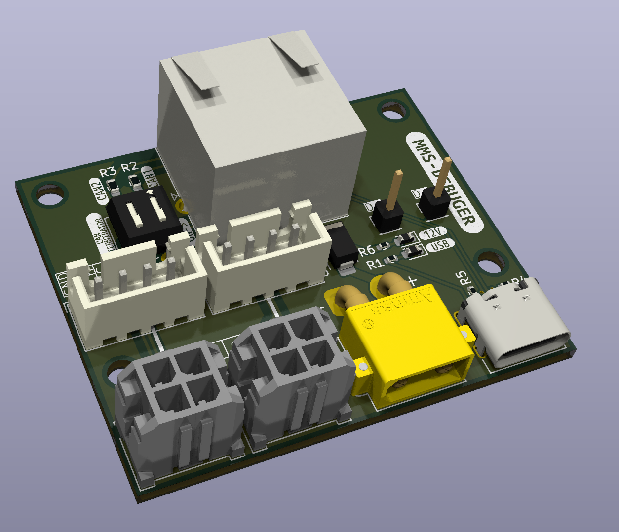
Debug can usb is an open-source printed circuit board by X-Lemon-X, from the X-Lemon-X/mms_debuger_board repository on GitHub, published under the MIT licence. It is a 2-layer board of 48 × 40 mm with 28 parts on 26 nets, routed with 133 tracks and 4 vias.
It is built around the SS34. Its parts include 7 connectors, 6 resistors, 3 diodes, 2 ICs and 1 switch.
| Pin | Function | Description |
|---|---|---|
| 1 | CAN1 L | CAN 1 Low speed up to 1 Mb/s |
| 2 | CAN1 H | CAN 1 High speed up to 1 Mb/s |
| 3 | GND | 500mA |
| 4 | CAN2 L | CAN 2 Low speed up to 5 Mb/s |
| 5 | CAN2 H | CAN 2 High speed up to 5 Mb/s |
| 6 | 12V | 500 mA |
| 7 | USB D- | USB data plus |
| 8 | USB D+ | USB data minus |
| Qty | Value | Footprint | References |
|---|---|---|---|
| 2 | 120R | Resistor_SMD:R_0603_1608Metric | R2, R3 |
| 2 | 4k7 | Resistor_SMD:R_0402_1005Metric | R4, R5 |
| 2 | CAN | Connector_Molex:Molex_Micro-Fit_3.0_43045-0412_2x02_P3.00mm_Vertical | U2, U3 |
| 2 | Conn_01x01_Pin | Connector_PinHeader_2.54mm:PinHeader_1x01_P2.54mm_Vertical | J4, J6 |
| 2 | Conn_01x04 | Connector_JST:JST_XH_B4B-XH-A_1x04_P2.50mm_Vertical | J1, J3 |
| 2 | G*** | kibuzzard-675D9C73 | kibuzzard-675D9C73, kibuzzard-675D9C73 |
| 2 | G*** | kibuzzard-675D9C7D | kibuzzard-675D9C7D, kibuzzard-675D9C7D |
| 2 | LV_PWR | Diode_SMD:D_0603_1608Metric | D1, D2 |
| 1 | 1k | Resistor_SMD:R_0402_1005Metric | R6 |
| 1 | 220 | Resistor_SMD:R_0402_1005Metric | R1 |
| 1 | Conn_01x02 | Connector_AMASS:AMASS_XT30PW-M_1x02_P2.50mm_Horizontal | J7 |
| 1 | G*** | kibuzzard-67840BAA | kibuzzard-67840BAA |
| 1 | G*** | kibuzzard-675D9CCD | kibuzzard-675D9CCD |
| 1 | G*** | kibuzzard-6784102F | kibuzzard-6784102F |
| 1 | G*** | kibuzzard-67840A5C | kibuzzard-67840A5C |
| 1 | G*** | kibuzzard-67840A66 | kibuzzard-67840A66 |
| 1 | RJ45_LED_Shielded | Connector_RJ:RJ45_Amphenol_RJHSE538X | J2 |
| 1 | SW_DIP_x02 | Button_Switch_THT:SW_DIP_SPSTx02_Slide_6.7x6.64mm_W7.62mm_P2.54mm_LowProfile | SW1 |
| 1 | USB_C_Receptacle_USB2.0 | Connector_USB:USB_C_Receptacle_G-Switch_GT-USB-7010ASV | J5 |
| 1 | ss34 | Diode_SMD:D_SMA | D3 |
willem-pennings/balancing-cube
A cube that balances itself in a corner or edge using reaction wheels

Arrow-air/project-quiver
Project Quiver documentation, designs, and project artifacts.


Arrow-air/project-caribou
Project Caribou documentation, designs, and project artifacts.

FujiNetWIFI/fujinet-hardware
Schematics and design files for FujiNet hardware


CrashOverride85/zc95
4 channel EStim box inspired by the mk312bt, with Lua scripting support

It measures 48 × 40 mm and has 2 copper layers, 1.6 mm thick.
28 parts, built around the SS34. The full list of its parts is on this page, with links to each part's symbol and footprint where PCBKit's library has them.
From the X-Lemon-X/mms_debuger_board repository on GitHub, at the commit this page was made from: the board is debug_can_usb/debug_can_usb.kicad_pcb and its schematic debug_can_usb/Power.kicad_sch. PCBKit opens the board in the browser, with nothing to install.
Its repository publishes it under the MIT licence: you may reuse it on that licence's terms (keep the author's notice, and for a copyleft licence share your changes alike).