2 layers174 × 58 mm
Breakout 112pin Connector
rusefi/rusefi
rusefi - GPL internal combustion engine control unit
42 parts1.2k
 Triver1/TSplit
Split keyboard design files
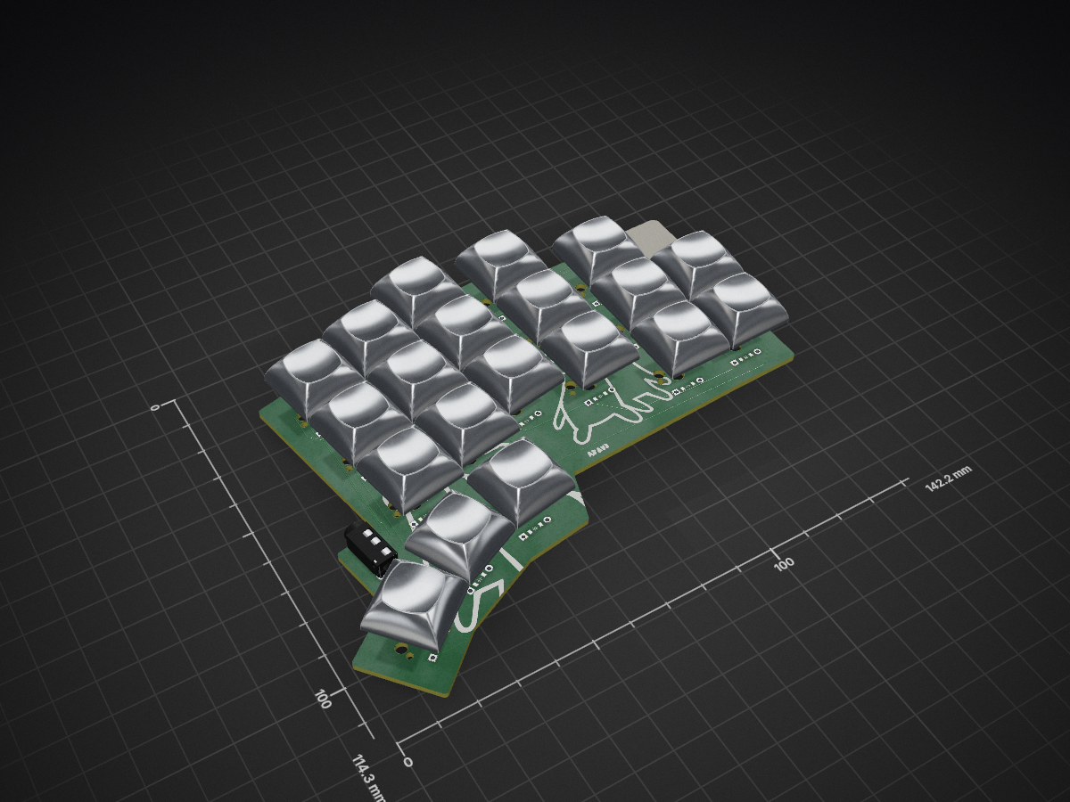
Left mapped is an open-source printed circuit board by Triver1, from the Triver1/TSplit repository on GitHub. It is a 2-layer board of 142.2 × 114.3 mm with 42 parts on 34 nets, routed with 365 tracks and 0 vias.
Its parts include 20 diodes and 20 switches. It belongs with the keyboards and input boards of this library.
| Qty | Value | Footprint | References |
|---|---|---|---|
| 20 | ComboDiode | D1, D2, D3, D4, D5, D10, D11, D12, D13, D14, D15, D16, D17, D18, D19, D20 +4 | |
| 20 | MX | S1, S2, S3, S4, S5, S10, S11, S12, S13, S14, S15, S16, S17, S18, S19, S20 +4 | |
| 1 | xiao-ble-tht | ||
| 1 | TRRS-PJ-320A-dual | TRRS-PJ-320A-dual | TRRS1 |
rusefi/rusefi
rusefi - GPL internal combustion engine control unit


hackclub/sprig
🍃 Learn to code by making games in a JavaScript web-based game editor.

jamro/tiny-engineer
A small desktop robot that brings an AI coding assistant to life, physically acting out when it reads files, thinks, writes code, and finishes work.

hoglet67/RGBtoHDMI
Bare-metal Raspberry Pi project that provides pixel-perfect sampling of Retro Computer RGB/YUV video and conversion to HDMI

hackclub/OnBoard
💡 Join 1,000 teenagers and make your first PCB with a $100 grant!


It measures 142.2 × 114.3 mm and has 2 copper layers, 1.6 mm thick.
42 parts. The full list of its parts is on this page, with links to each part's symbol and footprint where PCBKit's library has them.
From the Triver1/TSplit repository on GitHub, at the commit this page was made from: the board is output/pcbs/left_mapped.kicad_pcb. PCBKit opens the board in the browser, with nothing to install.
Its repository states no licence, so its author keeps all rights: ask Triver1 before reusing the design.