Skip to the content
2 layers100 × 100 mmElektronica 2 opstellingen, the printed circuit board in 3D

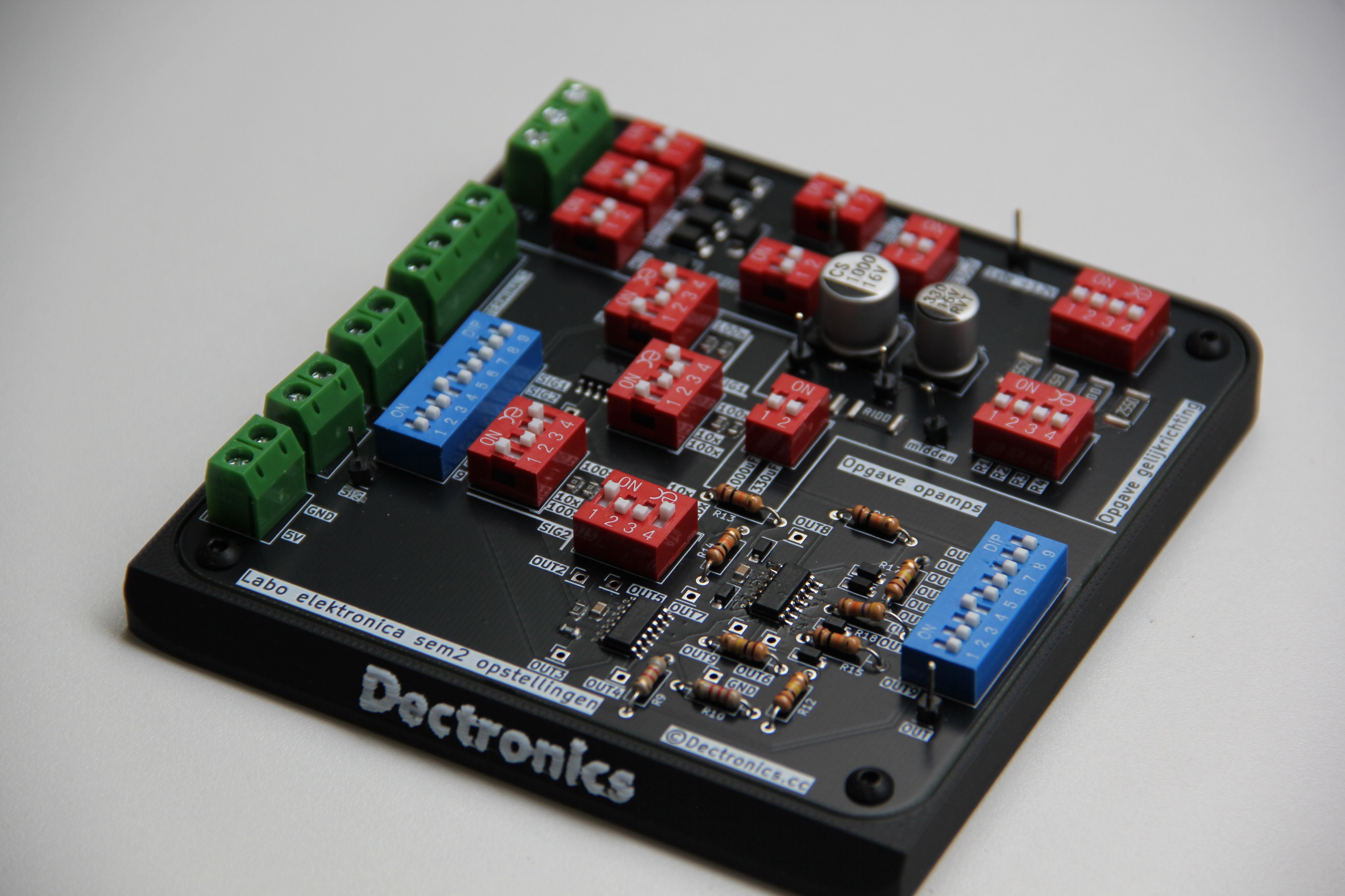
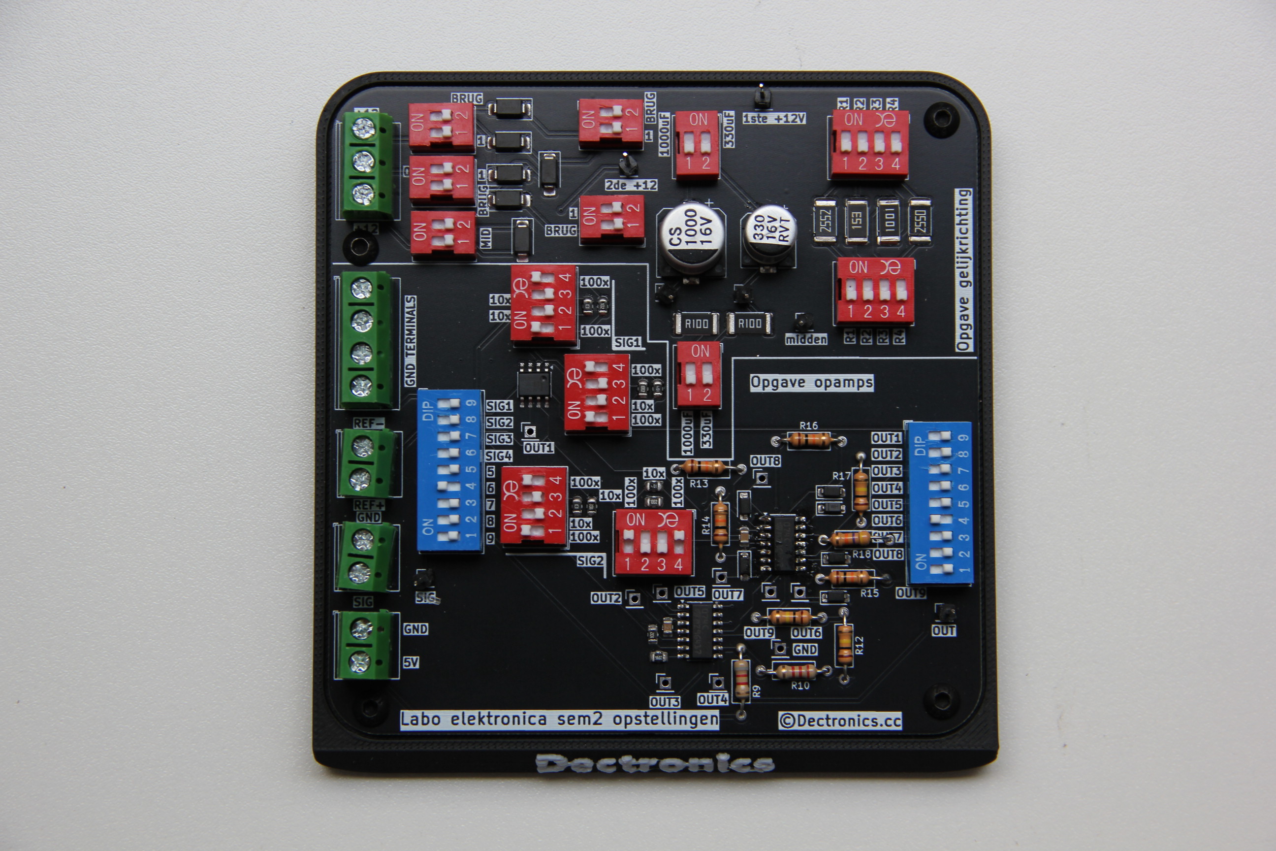
Complete printplaat met alle schakelingen van zowel gelijkrichting als opamps (Vives kortrijk)

Size
100 × 100 mm
Copper layers
2
Thickness
1.6 mm
Parts
86
Nets
83
Pads
266
Tracks, vias
515, 23
Pours
1
Routed
Yes
KiCad
KiCad 8.0 (file 20240108)
Created
21 May 2025
Updated
21 May 2025

Overview

Elektronica 2 opstellingen is an open-source printed circuit board by TiebeDeclercq, from the TiebeDeclercq/Elektronica2-Labo-Opstelling repository on GitHub, published under the MIT licence. It is a 2-layer board of 100 × 100 mm with 86 parts on 83 nets, routed with 515 tracks and 23 vias.

It is built around the US1M. Its parts include 22 connectors, 20 resistors, 15 switches, 12 diodes and 4 capacitors.

Main components

1

README

README.md

Elektronica2-Labo-Opstelling

Complete printplaat met alle schakelingen van zowel gelijkrichting als opamps @Vives kortrijk Met een printbare voet voor betere stabiliteit en geen kortsluiting te krijgen. Op deze voet wordt er gewerkt met heated inserts (M3) voor het monteren van de print.

Assembled PCB

Het schema is als volgt:

image

Voor het solderen kan je gebruikmaken van de meegeleverde BOM file, alle componenten zijn 0805 buiten sommige TH componenten (omdat deze eigen keuze zijn en makkelijk te verangen moeten zijn)

Assembled PCB

Parts

86
QtyValueFootprintReferences
17Conn_01x01_PinConnector_PinHeader_2.54mm:PinHeader_1x01_P2.54mm_VerticalJ5, J6, J7, J8, J10, J11, J12, J13, J14, J15, J16, J17, J18, J19, J20, J21 +1
8RResistor_THT:R_Axial_DIN0207_L6.3mm_D2.5mm_P10.16mm_HorizontalR11, R12, R13, R14, R15, R16, R17, R18
7SW_DIP_x02Button_Switch_THT:SW_DIP_SPSTx02_Slide_9.78x7.26mm_W7.62mm_P2.54mmSW3, SW4, SW5, SW6, SW7, SW8, SW9
6D_ZenerDiode_SMD:D_SOD-123D3, D4, D5, D6, D11, D12
6SW_DIP_x04Button_Switch_THT:SW_DIP_SPSTx04_Slide_9.78x12.34mm_W7.62mm_P2.54mmSW1, SW2, SW10, SW11, SW12, SW13
6US1MDiode_SMD:D_SMAD1, D2, D7, D8, D9, D10
4MountingHoleMountingHole:MountingHole_3.2mm_M3H1, H2, H3, H4
31kResistor_SMD:R_0805_2012MetricR7, Ri1, Ri3
3Screw_Terminal_01x02TerminalBlock_Phoenix:TerminalBlock_Phoenix_MKDS-1,5-2_1x02_P5.00mm_HorizontalJ2, J4, J22
20,1Ω, 1WResistor_SMD:R_2512_6332MetricR5, R6
2100Resistor_SMD:R_0805_2012MetricRi2, Ri4
2100kResistor_SMD:R_0805_2012MetricRf2, Rf3
2100nFCapacitor_SMD:C_0805_2012MetricC3, C4
210kResistor_SMD:R_0805_2012MetricRf1, Rf4
2SW_DIP_x09Button_Switch_THT:SW_DIP_SPSTx09_Slide_9.78x25.04mm_W7.62mm_P2.54mmSW14, SW15
2TL074Package_SO:SOIC-14_3.9x8.7mm_P1.27mmU2, U3
11000uFCapacitor_SMD:CP_Elec_10x10.5C1
114kΩ, 1WResistor_SMD:R_2512_6332MetricR2
12,5kΩ, 1WResistor_SMD:R_2512_6332MetricR3
125kΩ, 1WResistor_SMD:R_2512_6332MetricR1
12kResistor_THT:R_Axial_DIN0207_L6.3mm_D2.5mm_P10.16mm_HorizontalR10
1330uFCapacitor_SMD:CP_Elec_8x10C2
155Ω, 1WResistor_SMD:R_2512_6332MetricR4
18kResistor_THT:R_Axial_DIN0207_L6.3mm_D2.5mm_P10.16mm_HorizontalR9
199kResistor_SMD:R_0805_2012MetricR8
1LM741Package_SO:SOIC-8_3.9x4.9mm_P1.27mmU1
1Screw_Terminal_01x03TerminalBlock_Phoenix:TerminalBlock_Phoenix_MKDS-1,5-3_1x03_P5.00mm_HorizontalJ1
1Screw_Terminal_01x04TerminalBlock_Phoenix:TerminalBlock_Phoenix_MKDS-1,5-4-5.08_1x04_P5.08mm_HorizontalJ3

Similar boards

  • 4 layers75.2 × 99.5 mmFOC, the printed circuit board in 3D

    FOC

    nordstream3/FOC

    Date | Manufacturer | amount | includes | shipping & tax | price | -------- | -------- | -------- | -------- | -------- | -------- | 2024-01-17 | JLCPCB | 10 boards | All assembled excl fets and caps | YES, to EU |…

    261 parts81
  • 2 layers140.7 × 47.4 mmEG8010 A1, the printed circuit board in 3D

    EG8010 A1

    Millisman/EG8010

    Collection of designs for the EG8010 (ASIC for single-phase SPWM control H-bridge)

    201 parts17MIT
  • 2 layers31.2 × 53.3 mmNanit, the printed circuit board in 3D

    Nanit

    andykarpov/nanit

    Alternate PCB for NANIT project https://radiokot.ru/circuit/digital/measure/117/

    73 parts7
  • 2 layers50 × 51 mmPrismo reader, the printed circuit board in 3D

    Prismo reader

    hacklabkyiv/prismo-reader

    RFID readers of Prismo access management system

    48 parts5GPL-3.0
  • 2 layers37 × 90 mmESP32-BLE GSM, the printed circuit board in 3D

    ESP32-BLE GSM

    shridattdudhat/ESP01-MOSFET-Control

    Control LED or DC Motor using ESP-01!

    43 parts5
  • 2 layersEcu, the printed circuit board in 3D

    Ecu

    felipeschmitt04/ecu-pic16f877a

    Academic ECU project in C for the PIC16F877A, with Proteus simulation and KiCad PCB design.

    77 parts4
  • 2 layers89 × 44 mmCDRC, the printed circuit board in 3D

    CDRC

    lilindian16/customDRC

    Development of custom Audison DRC interface

    85 parts4
  • 2 layers137 × 84 mmESP32-Geiger Counter, the printed circuit board in 3D

    ESP32-Geiger Counter

    AronASzucs/Avalanche32

    Handheld ESP32-S3 Geiger counter with a firmware-regulated 400 V boost, SBM-20 tube, USB-C charging and OLED display.

    89 parts3

Questions

How big is the Elektronica 2 opstellingen PCB?

It measures 100 × 100 mm and has 2 copper layers, 1.6 mm thick.

What parts does the Elektronica 2 opstellingen use?

86 parts, built around the US1M. The full list of its parts is on this page, with links to each part's symbol and footprint where PCBKit's library has them.

Where can I download the Elektronica 2 opstellingen KiCad files?

From the TiebeDeclercq/Elektronica2-Labo-Opstelling repository on GitHub, at the commit this page was made from: the board is Elektronica 2 opstellingen/Elektronica 2 opstellingen.kicad_pcb and its schematic Elektronica 2 opstellingen/Elektronica 2 opstellingen.kicad_sch. PCBKit opens the board in the browser, with nothing to install.

Can I use the Elektronica 2 opstellingen design in my own project?

Its repository publishes it under the MIT licence: you may reuse it on that licence's terms (keep the author's notice, and for a copyleft licence share your changes alike).