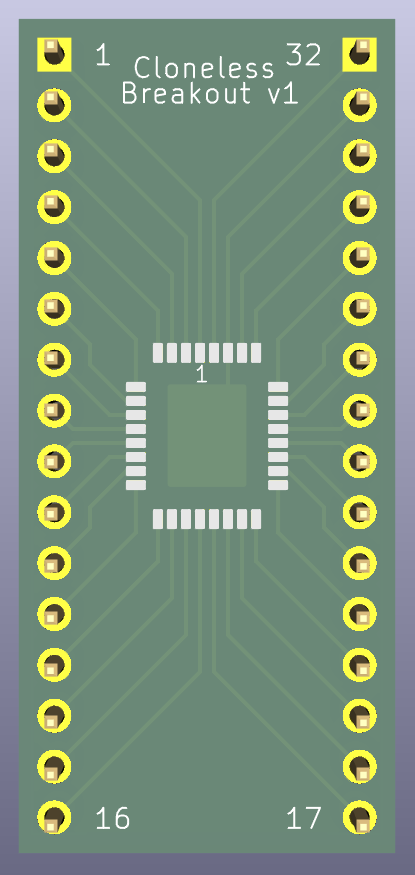
2 layers18.8 × 41.7 mm
Cloneless breakout v1
ThorbenMoos/Cloneless_artifacts
PCB designs, FPGA controllers, verification collateral and software artifacts related to the Cloneless series of tamper-resistant open-source ASICs
3 partsGPL-3.0

 ThorbenMoos/Cloneless_artifacts
PCB designs, FPGA controllers, verification collateral and software artifacts related to the Cloneless series of tamper-resistant open-source ASICs
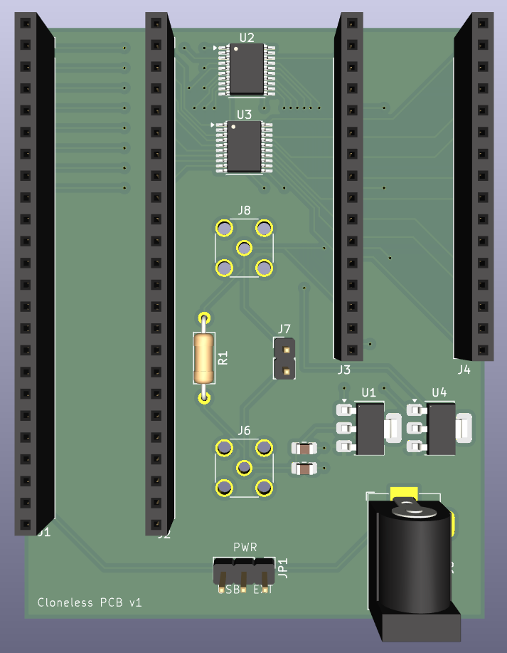
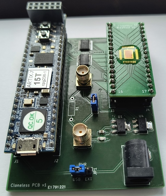
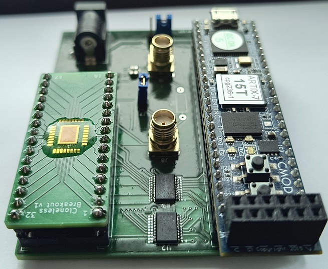
Cloneless pcb v1 is an open-source printed circuit board by ThorbenMoos, from the ThorbenMoos/Cloneless_artifacts repository on GitHub, published under the GPL-3.0 licence. It is a 2-layer board of 58.5 × 75 mm with 16 parts on 70 nets, routed with 234 tracks and 37 vias.
It is built around the TXS0108EPW, AMS1117-3.3 and AMS1117-5.0. Its parts include 8 connectors, 4 ICs, 2 capacitors and 1 resistor.


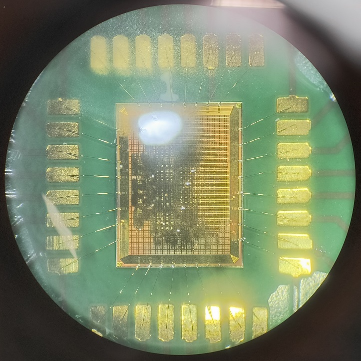
This repository contains PCB designs, FPGA controllers, verification collateral and software artifacts related to the Cloneless series of tamper-resistant open-source ASICs, in particular the Cloneless1 and Cloneless2 chips.
| Qty | Value | Footprint | References |
|---|---|---|---|
| 2 | Conn_01x16 | Connector_PinSocket_2.54mm:PinSocket_1x16_P2.54mm_Vertical | J3, J4 |
| 2 | Conn_01x24 | Connector_PinSocket_2.54mm:PinSocket_1x24_P2.54mm_Vertical | J1, J2 |
| 2 | Conn_Coaxial_Small | Connector_Coaxial:SMA_Wurth_60312002114503_Vertical | J6, J8 |
| 2 | TXS0108EPW | Package_SO:TSSOP-20_4.4x6.5mm_P0.65mm | U2, U3 |
| 1 | 100nF | Capacitor_SMD:C_0805_2012Metric_Pad1.18x1.45mm_HandSolder | C2 |
| 1 | 10µF | Capacitor_SMD:C_0805_2012Metric_Pad1.18x1.45mm_HandSolder | C1 |
| 1 | 1Ω | Resistor_THT:R_Axial_DIN0207_L6.3mm_D2.5mm_P10.16mm_Horizontal | R1 |
| 1 | AMS1117-3.3 | Package_TO_SOT_SMD:SOT-223-3_TabPin2 | U4 |
| 1 | AMS1117-5.0 | Package_TO_SOT_SMD:SOT-223-3_TabPin2 | U1 |
| 1 | Barrel_Jack_Switch | Connector_BarrelJack:BarrelJack_Horizontal | J5 |
| 1 | Conn_01x02 | Connector_PinHeader_2.54mm:PinHeader_1x02_P2.54mm_Vertical | J7 |
| 1 | Jumper_3_Open | Connector_PinHeader_2.54mm:PinHeader_1x03_P2.54mm_Vertical | JP1 |
ThorbenMoos/Cloneless_artifacts
PCB designs, FPGA controllers, verification collateral and software artifacts related to the Cloneless series of tamper-resistant open-source ASICs

practable/truss
The truss remote laboratory has been designed for use with Structural Engineering and Engineering Design courses at the University of Edinburgh.

Shubham-Khandelwal1/Universal-Robotic-Arm-Driver
The architecture follows a per-joint control philosophy, where each PCB operates as an independent node responsible for motor control and feedback acquisition, while communicating with a central compute unit (Jetson).

Ruthvik-reddy-A/PCB-design-projects
Welcome to my curated collection of hardware design projects focused on practical, compact, and beginner-to-intermediate level printed circuit board (PCB) designs.

MetalMusings/MyOwnEtherCATDevice
Documentation accompanying the "Make My Own EtherCAT device" video serie on Youtube.

kvazimoda24/TionO2-ZigBee
Ядром проекта является микроконтроллер ATmega328P. Для работы по протоколу ZigBee используется модуль E18-MS1-PCB.

galopago/din-rail-circuits
Collection of electronic circuits for DIN RAIL mount


It measures 58.5 × 75 mm and has 2 copper layers, 1.6 mm thick.
16 parts, built around the TXS0108EPW, AMS1117-3.3 and AMS1117-5.0. The full list of its parts is on this page, with links to each part's symbol and footprint where PCBKit's library has them.
From the ThorbenMoos/Cloneless_artifacts repository on GitHub, at the commit this page was made from: the board is PCB_designs/cloneless_pcb_v1/cloneless_pcb_v1.kicad_pcb and its schematic PCB_designs/cloneless_breakout_v1/cloneless_breakout_v1.kicad_sch. PCBKit opens the board in the browser, with nothing to install.
Its repository publishes it under the GPL-3.0 licence: you may reuse it on that licence's terms (keep the author's notice, and for a copyleft licence share your changes alike).