2 layers95.5 × 52 mm
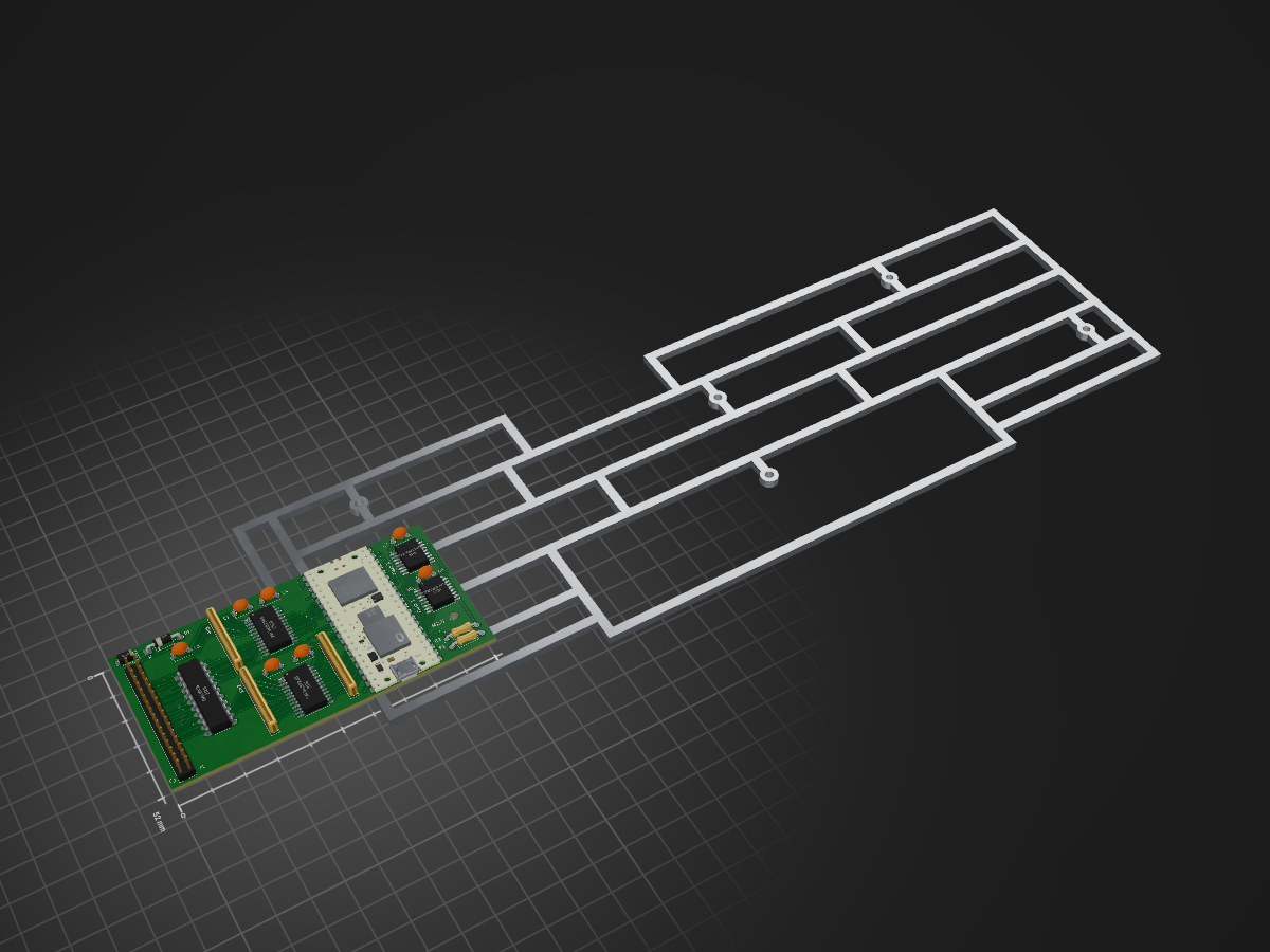
 ThomasFok/MegaFlash20
MegaFlash for Apple IIc/IIc+ computer
Megaflash is an open-source printed circuit board by ThomasFok, from the ThomasFok/MegaFlash repository on GitHub, published under the MIT licence. It is a 2-layer board of 102 × 52 mm with 22 parts on 78 nets, routed with 563 tracks and 67 vias.
It is built around the W25Q01JVSFIM, 74LVC8T245PW and SS12. Its parts include 7 capacitors, 6 ICs, 2 resistors, 2 diodes and 1 connector. It belongs with the RP2040 and FPGA and CPLD boards of this library.


| Qty | Value | Footprint | References |
|---|---|---|---|
| 7 | 0.1u | Capacitor_THT:C_Disc_D5.1mm_W3.2mm_P5.00mm | C1, C2, C3, C4, C5, C6, C7 |
| 3 | 100k | Resistor_THT:R_Array_SIP9 | RN1, RN2, RN3 |
| 2 | 100k | Resistor_THT:R_Axial_DIN0207_L6.3mm_D2.5mm_P10.16mm_Horizontal | R1, R2 |
| 2 | 74LVC8T245 | Package_SO:SOIC-24W_7.5x15.4mm_P1.27mm | U1, U2 |
| 2 | W25Q01JVSF | Package_SO:SOIC-16W_7.5x10.3mm_P1.27mm | U5, U6 |
| 1 | 1N5817 | Diode_THT:D_DO-41_SOD81_P10.16mm_Horizontal | D1 |
| 1 | EXPSLOT | misc:PinHeader_2x17_P2.54mm_Vertical_Mirror | J1 |
| 1 | GAL16V8 | Package_DIP:DIP-20_W7.62mm_LongPads | U3 |
| 1 | MountingHole | MountingHole:MountingHole_2.7mm_M2.5 | H1 |
| 1 | Pico | MCU_RaspberryPi_and_Boards:RPi_Pico_SMD_NO_LABEL_NO_DEBUG | U4 |
| 1 | SS12 | Diode_SMD:D_SMA | D2 |


It measures 102 × 52 mm and has 2 copper layers, 1.6 mm thick.
22 parts, built around the W25Q01JVSFIM, 74LVC8T245PW and SS12. The full list of its parts is on this page, with links to each part's symbol and footprint where PCBKit's library has them.
From the ThomasFok/MegaFlash repository on GitHub, at the commit this page was made from: the board is kicad/rev1.1b/megaflash.kicad_pcb and its schematic kicad/rev1.0/megaflash.kicad_sch. PCBKit opens the board in the browser, with nothing to install.
Its repository publishes it under the MIT licence: you may reuse it on that licence's terms (keep the author's notice, and for a copyleft licence share your changes alike).

