

4 layers254.9 × 150.1 mm

 TheodorosBalis/Mixed-Signal-PCB1
Four-layer KiCad PCB for a GSM/GPRS handheld with STM32, Quectel M95, battery charging, LCD, SIM, keypad, and audio.
MixedsignalBoard is an open-source printed circuit board by TheodorosBalis, from the TheodorosBalis/Mixed-Signal-PCB repository on GitHub. It is a 4-layer board of 46 × 100 mm with 123 parts on 101 nets, routed with 1,046 tracks and 143 vias.
It is built around the BQ24166RGER, BC846 and BAT54, with the ESD9B3.3ST5G, PESD3V3S1UL and SP0504BAJTG among its other parts. Its parts include 45 capacitors, 25 resistors, 20 switches, 9 diodes and 6 connectors. It belongs with the keyboards and input and audio and music boards and the STM32 boards of this library.


A four-layer KiCad 9 PCB design for a compact GSM/GPRS handheld device. It combines a Quectel M95 cellular module, an STM32 microcontroller, battery charging and regulation, a SIM interface, display connector, keypad, and audio circuitry.
| Item | Implemented design |
|---|---|
| Board outline | 46 x 100 mm |
| Copper layers | 4: F.Cu, In1.Cu, In2.Cu, B.Cu |
| Stackup material | FR-4 dielectrics; ENIG finish specified in KiCad |
| Board thickness | 2.9984 mm as currently stored in the PCB file; confirm with the fabricator |
| Cellular module | Quectel M95 GSM/GPRS (U1) |
| MCU | STM32G030K6Tx (U2) |
| Power | BQ24166RGE charger/power-path IC (U4), 3.3 V regulator (U3), Micro-USB power input (J3), battery connector (J1) |
| RF interface | U.FL coaxial connector (J6) for an external antenna; 0-ohm series link (R5) and DNP shunt matching positions (C16, C17) |
| Display | 12-position, 0.5 mm-pitch FPC connector (J4) for the intended ST7789-based 240 x 240 LCD module |
| SIM | Nano-SIM connector (J5) with interface protection |
| User I/O | 20 keypad switches, status LEDs, microphone, speaker |
| Programming/debug | Tag-Connect SWD connector (J2); SWO is not connected |
| Mechanical | Four 2 mm mounting-hole footprints |
The Micro-USB connector is used for power; its USB data pins are unconnected in this design. The U.FL connector is not an antenna: an appropriate external antenna and cable are required for RF operation.
mixedsignalBoard.kicad_pro - KiCad project settings.mixedsignalBoard.kicad_sch - circuit schematic.mixedsignalBoard.kicad_pcb - PCB layout, footprints, routing, and board stackup.Open mixedsignalBoard.kicad_pro with KiCad 9 to inspect the schematic and layout. Firmware, manufacturing exports, assembly files, and a physical antenna are not included in this repository.
This is a design project, not a validated hardware product. Check the actual LCD module pinout and connector orientation, antenna matching and 50-ohm RF geometry against the chosen fabricator's stackup, and all component part numbers before ordering. The PCB currently assigns both inner copper zones to M95_SIM_GND and records an approximately 3.0 mm stackup; verify that these are intentional and manufacturable. Passing ERC or DRC alone does not establish electrical, RF, or functional performance.
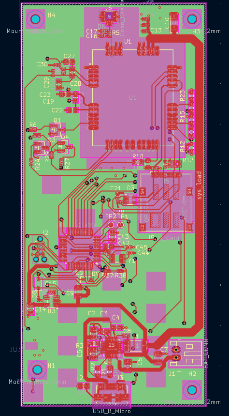
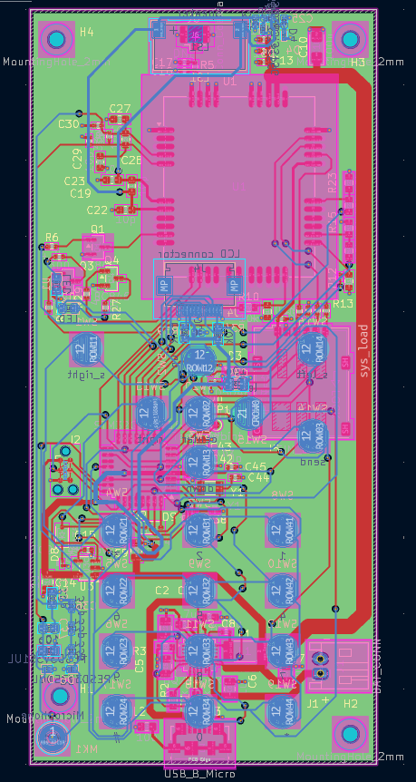
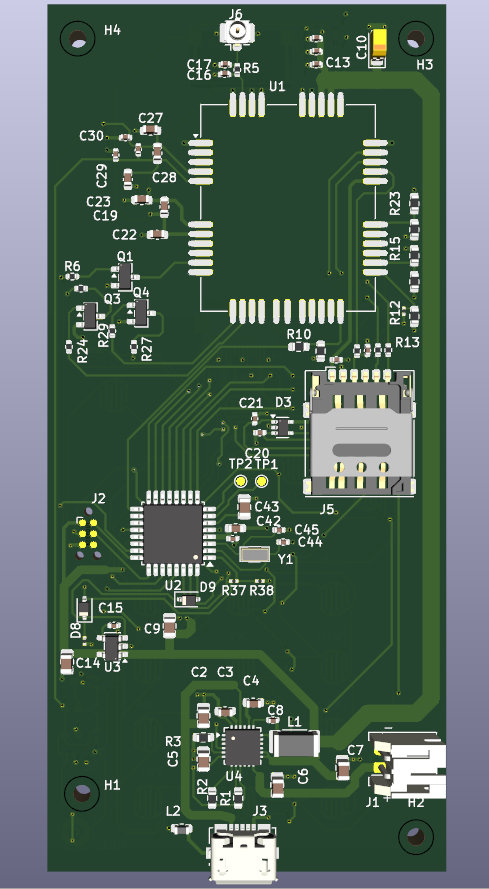
The views below show the system block diagram, complete schematic, PCB routing, and both sides of the board. The 3D images are KiCad renders, not photographs of fabricated hardware.
The diagram summarizes power distribution and the connections between the STM32, M95, display, keypad, SIM, RF, and audio circuits.
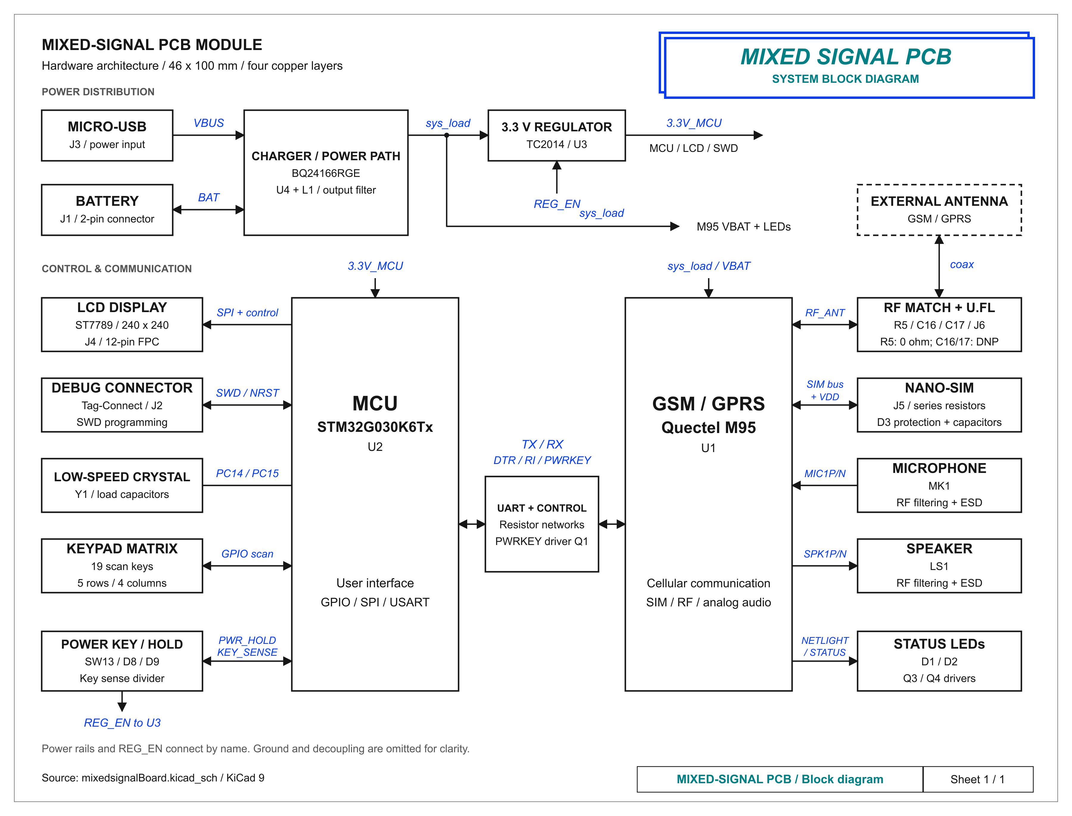
High-resolution PNG | Editable SVG
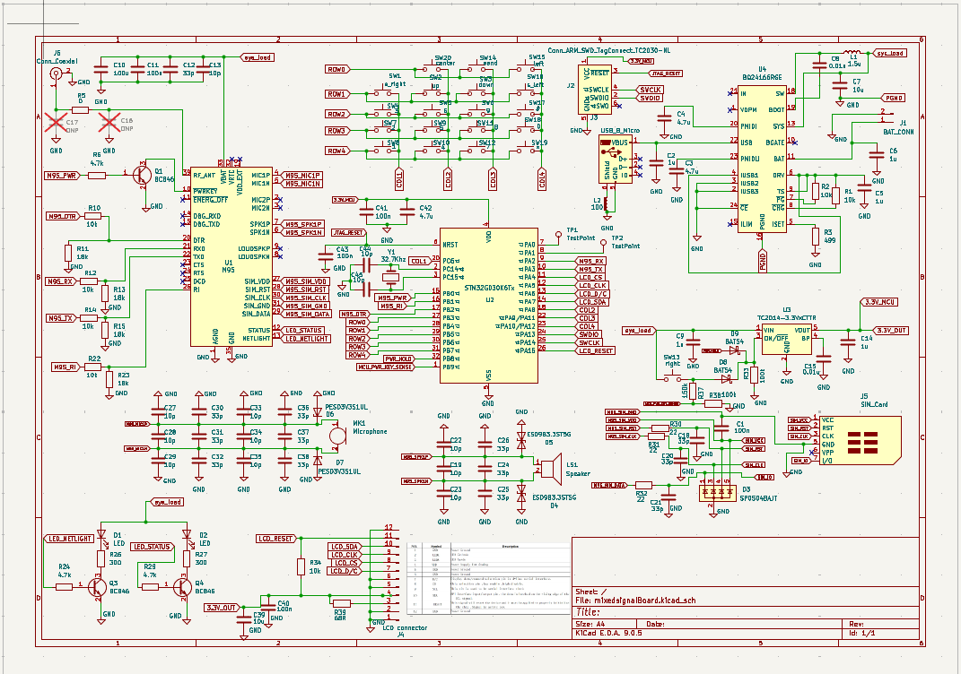
| Front copper view | Multi-layer routing view |
|---|---|
 |  |
| Component side | Keypad side |
|---|---|
 | 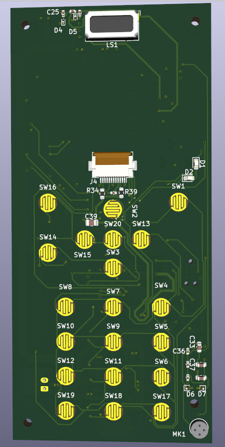 |
| Perspective view | Board edge profile |
|---|---|
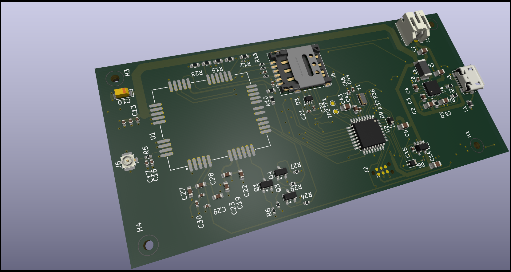 | 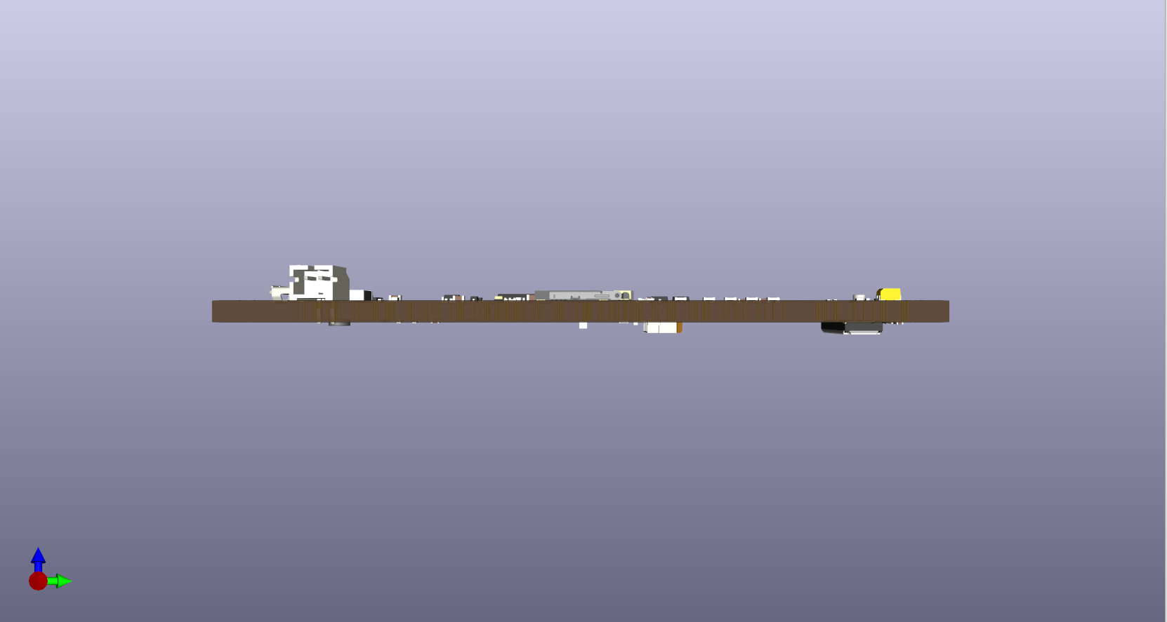 |
| Qty | Value | Footprint | References |
|---|---|---|---|
| 13 | 33p | Capacitor_SMD:C_0402_1005Metric | C12, C18, C20, C21, C24, C25, C26, C30, C31, C32, C36, C37, C38 |
| 9 | 10p | Capacitor_SMD:C_0603_1608Metric | C19, C22, C23, C27, C28, C29, C33, C34, C35 |
| 6 | 10k | Resistor_SMD:R_0603_1608Metric | R1, R2, R10, R14, R22, R34 |
| 5 | 1u | Capacitor_SMD:C_0805_2012Metric | C2, C5, C6, C9, C14 |
| 4 | 100n | Capacitor_SMD:C_0402_1005Metric | C1, C11, C40, C41 |
| 4 | 18k | Resistor_SMD:R_0603_1608Metric | R11, R13, R15, R23 |
| 4 | MountingHole_2mm | MountingHole:MountingHole_2mm | H1, H2, H3, H4 |
| 3 | 10p | Capacitor_SMD:C_0402_1005Metric | C13, C44, C45 |
| 3 | 22 | Resistor_SMD:R_0402_1005Metric | R30, R31, R32 |
| 3 | 4.7k | Resistor_SMD:R_0402_1005Metric | R6, R24, R29 |
| 3 | 4.7u | Capacitor_SMD:C_0603_1608Metric | C3, C4, C42 |
| 3 | BC846 | Package_TO_SOT_SMD:SOT-23 | Q1, Q3, Q4 |
| 2 | 0.01u | Capacitor_SMD:C_0402_1005Metric | C8, C15 |
| 2 | 100k | Resistor_SMD:R_0201_0603Metric | R33, R38 |
| 2 | 10u | Capacitor_SMD:C_0805_2012Metric | C7, C39 |
| 2 | 300 | Resistor_SMD:R_0402_1005Metric | R26, R27 |
| 2 | BAT54 | Diode_SMD:D_SOD-323 | D8, D9 |
| 2 | DNP | Capacitor_SMD:C_0402_1005Metric | C16, C17 |
| 2 | ESD9B3.3ST5G | Diode_SMD:D_SOD-923 | D4, D5 |
| 2 | LED | LED_SMD:LED_0603_1608Metric | D1, D2 |
| 2 | PESD3V3S1UL | Diode_SMD:D_SOD-882 | D6, D7 |
| 2 | TestPoint | TestPoint:TestPoint_Pad_D1.0mm | TP1, TP2 |
| 1 | # | Button_Switch_SMD:membrane_switch_4.4mm_V2 | SW17 |
| 1 | * | Button_Switch_SMD:membrane_switch_4.4mm_V2 | SW19 |
| 1 | 0 | Button_Switch_SMD:membrane_switch_4.4mm_V2 | SW18 |
| 1 | 0 | Resistor_SMD:R_0402_1005Metric | R5 |
| 1 | 1 | Button_Switch_SMD:membrane_switch_4.4mm_V2 | SW8 |
| 1 | 1.5u | Inductor_SMD:L_2010_5025Metric | L1 |
| 1 | 100 | Inductor_SMD:L_0603_1608Metric | L2 |
| 1 | 100n | Capacitor_SMD:C_0805_2012Metric | C43 |
| 1 | 100u | Capacitor_Tantalum_SMD:CP_EIA-3216-18_Kemet-A | C10 |
| 1 | 10k | Resistor_SMD:R_0201_0603Metric | R12 |
| 1 | 150k | Resistor_SMD:R_0201_0603Metric | R37 |
| 1 | 2 | Button_Switch_SMD:membrane_switch_4.4mm_V2 | SW7 |
| 1 | 3 | Button_Switch_SMD:membrane_switch_4.4mm_V2 | SW4 |
| 1 | 32.7Khz | Crystal:Crystal_SMD_3215-2Pin_3.2x1.5mm | Y1 |
| 1 | 4 | Button_Switch_SMD:membrane_switch_4.4mm_V2 | SW10 |
| 1 | 499 | Resistor_SMD:R_0603_1608Metric | R3 |
| 1 | 5 | Button_Switch_SMD:membrane_switch_4.4mm_V2 | SW9 |
| 1 | 6 | Button_Switch_SMD:membrane_switch_4.4mm_V2 | SW5 |
| 1 | 68R | Resistor_SMD:R_0603_1608Metric | R39 |
| 1 | 7 | Button_Switch_SMD:membrane_switch_4.4mm_V2 | SW12 |
| 1 | 8 | Button_Switch_SMD:membrane_switch_4.4mm_V2 | SW11 |
| 1 | 9 | Button_Switch_SMD:membrane_switch_4.4mm_V2 | SW6 |
| 1 | BAT_CONN | Connector_JST:JST_PH_S2B-PH-K_1x02_P2.00mm_Horizontal | J1 |
| 1 | BQ24166RGE | Package_DFN_QFN:Texas_RGE0024H_VQFN-24-1EP_4x4mm_P0.5mm_EP2.7x2.7mm | U4 |
| 1 | Conn_ARM_SWD_TagConnect_TC2030-NL | Connector:Tag-Connect_TC2030-IDC-NL_2x03_P1.27mm_Vertical | J2 |
| 1 | Conn_Coaxial | Connector_Coaxial:U.FL_Hirose_U.FL-R-SMT-1_Vertical | J6 |
| 1 | LCD connector | Connector_FFC-FPC:Hirose_FH12-12S-0.5SH_1x12-1MP_P0.50mm_Horizontal | J4 |
| 1 | M95 | RF_GSM:Quectel_M95 | U1 |
| 1 | Microphone | Sensor_Audio:CUI_CMC-4013-SMT | MK1 |
| 1 | SIM_Card | Connector_Card:nanoSIM_Hinged_CUI_NSIM-2-C | J5 |
| 1 | SP0504BAJT | Package_TO_SOT_SMD:SOT-353_SC-70-5 | D3 |
| 1 | STM32G030K6Tx | Package_QFP:LQFP-32_7x7mm_P0.8mm | U2 |
| 1 | Speaker | Buzzer_Beeper:Speaker_CUI_CMR-1206S-67 | LS1 |
| 1 | TC2014-3.3VxCTTR | Package_TO_SOT_SMD:SOT-23-5 | U3 |
| 1 | USB_B_Micro | USB:USB_Micro-B_Molex_47346-0001 | J3 |
| 1 | center | Button_Switch_SMD:membrane_switch_4.4mm_V2 | SW20 |
| 1 | down | Button_Switch_SMD:membrane_switch_4.4mm_V2 | SW3 |
| 1 | left | Button_Switch_SMD:membrane_switch_4.4mm_V2 | SW15 |
| 1 | right | Button_Switch_SMD:membrane_switch_4.4mm_V2 | SW13 |
| 1 | s_left | Button_Switch_SMD:membrane_switch_4.4mm_V2 | SW16 |
| 1 | s_right | Button_Switch_SMD:membrane_switch_4.4mm_V2 | SW1 |
| 1 | send | Button_Switch_SMD:membrane_switch_4.4mm_V2 | SW14 |
| 1 | up | Button_Switch_SMD:membrane_switch_4.4mm_V2 | SW2 |


HearnChristian/atmos-sense
ESP32-based atmospheric sensing node: BME280 environmental sensing and AS3935 lightning detection over I2C, designed for drone integration. KiCad hardware plus firmware.
It measures 46 × 100 mm and has 4 copper layers, 3 mm thick.
123 parts, built around the BQ24166RGER, BC846, BAT54 and ESD9B3.3ST5G. The full list of its parts is on this page, with links to each part's symbol and footprint where PCBKit's library has them.
From the TheodorosBalis/Mixed-Signal-PCB repository on GitHub, at the commit this page was made from: the board is mixedsignalBoard.kicad_pcb and its schematic mixedsignalBoard.kicad_sch. PCBKit opens the board in the browser, with nothing to install.
Its repository states no licence, so its author keeps all rights: ask TheodorosBalis before reusing the design.