2 layers100 × 100 mm

 Shmerlard/SH818
a custom 16bit cpu
Register File Manager is an open-source printed circuit board by Shmerlard, from the Shmerlard/SH8 repository on GitHub. It is a 2-layer board of 100 × 100 mm with 48 parts on 72 nets, routed with 594 tracks and 12 vias.
It is built around the 74LS245SC, 74LS04PC and 74LS157PC. Its parts include 25 connectors, 7 ICs, 4 resistors, 4 diodes and 1 switch.


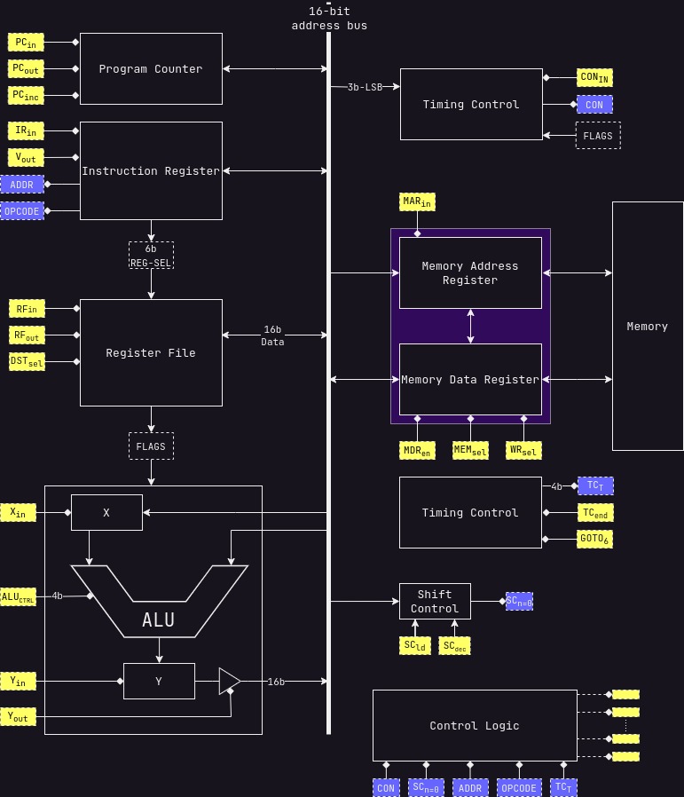
hi, my name is elad and Im an electrical engineering student in Ben gurion university. I designed a small 16bit cpu, with a mix of jdh8, src, msp430 and the Hack computer. this is still a work in progress, but so far it works.
I used logisim for the logic design, draw.io for the diagrams.
in order to see the working cpu in logisim: you need to build version 3.9.0 from source here, then just open the .circ file.
0x00:  NOP
0x01:  MOV  Ra/#, Rb       | Ra/# -> Rb
0x02:  ST   Ra/#, Rb/#     | Ra/# -> M[Rb]/
0x03:  PUSH Ra/#           | Ra/# -> @SP; SP--
0x04:  POP  Ra             | SP++; @SP -> Ra
0x05:  ADD  Ra/#, Rb       | Ra/# + Rb -> Rb
0x06:  ADDC Ra/#, Rb       | Ra/# + Rb + c -> Rb
0x07:  SUB  Ra/#, Rb       | Rb - Ra/# -> Rb
0x08:  CMP  Ra/#, Rb       | Rb - Ra/#
0x09:  SHR  Ra/#, Rb       | SHR Rb (Ra/# times) -> Rb
0x0A:  SHL
0x0B:  RRC  Ra/#, Rb       | RRC Rb (Ra/# times) -> Rb
0x0C:  RLC
0x0D:  AND  Ra/#, Rb       | Ra/# AND Rb -> Rb
0x0E:  OR   Ra/#, Rb       | Ra/# OR  Rb -> Rb
0x0F:  XOR  Ra/#, Rb       | Ra/# XOR Rb -> Rb
0x10:  NOT
0x11:  CALL DST            | PC -> @SP; DST -> PC; SP-- -> SP;
0x12:  RET
0x13:  JMP  DST            | DST -> PC
for more simulated instructions see: Simulated Instructions
0: SP/REG0  : STACK pointer
1: SR/REG1  : Status register
2: REG2     : GP Input
3: REG3     : GP Output
4: REG3     : GP
5: REG4     : GP
6: REG5     : GP
7: REG6 : GPthe memory ranges from 0x0000 to 0xFFFF.
the memory is mapped in the following way:
0x0000 - 0x7FFF: GP ROM              (32KiB    ROM)
0x8000 - 0xBFFF: GP RAM              (16KiB    RAM)
0xC000 - 0xCFFF: VRAM                (4KiB    RAM) #CURRENTLY NOT IN USE#
0xD000 - 0xFFFF: NOT IN USE (12KiB UNUSED)The instruction register is a 16-bit register
the format is XXXX-XUMM-SSSS-DDDD
X = the opcode of the instruction
U = Currently not in use
M = indicates the addressing mode
S = indicates the source register
D = indicates the destination register
(see addressing modes) for more info
for the full gallery go to Gallery
| Qty | Value | Footprint | References |
|---|---|---|---|
| 18 | Conn_01x02_Socket | Connector_JST:JST_XH_S2B-XH-A-1_1x02_P2.50mm_Horizontal | J4, J5, J6, J7, J10, J11, J12, J13, J14, J15, J16, J17, J18, J19, J20, J25 +2 |
| 4 | 1k | Resistor_SMD:R_1206_3216Metric_Pad1.30x1.75mm_HandSolder | R1, R2, R3, R4 |
| 4 | 74LS138 | Package_DIP:DIP-16_W7.62mm_Socket_LongPads | U2, U3, U4, U5 |
| 4 | Conn_01x08_Socket | Connector_PinHeader_2.54mm:PinHeader_1x08_P2.54mm_Vertical | J21, J22, J23, J24 |
| 4 | LED | LED_THT:LED_Rectangular_W3.0mm_H2.0mm | D1, D2, D3, D4 |
| 4 | MountingHole_Pad | MountingHole:MountingHole_2.2mm_M2_DIN965_Pad | H1, H2, H3, H4 |
| 3 | TestPoint | TestPoint:TestPoint_Pad_D1.0mm | TP1, TP2, TP3 |
| 2 | Conn_01x04_Socket | Connector_JST:JST_XH_S4B-XH-A-1_1x04_P2.50mm_Horizontal | J1, J2 |
| 1 | 74LS04 | Package_DIP:DIP-14_W7.62mm_Socket_LongPads | U6 |
| 1 | 74LS157 | Package_DIP:DIP-16_W7.62mm_Socket_LongPads | U1 |
| 1 | 74LS245 | Package_DIP:DIP-20_W7.62mm_Socket_LongPads | U7 |
| 1 | Conn_01x03_Socket | Connector_JST:JST_XH_S3B-XH-A-1_1x03_P2.50mm_Horizontal | J3 |
| 1 | SW_SPDT | Button_Switch_THT:SW_Slide_SPDT_Angled_CK_OS102011MA1Q | SW1 |


Nakazoto/CenturionComputer
This is just a simple backup of all the files related to the Centurion that I have stored on my HD. The Wiki itself has far more in-depth information about the Centurion and it's individual cards.

The-Invent0r/8-bit-Computer-PCB
These are the KiCAD files for my 8-Bit Computer.

btb/80ColumnCard
An Apple II 80-Column Card. Based on the Videx Videoterm


clemarfolly/Microdigital-TK2000
Reprodução da PCB do TK-2000 da Microdigital, clone do Micro-Professor MPF-II

rraider/Seminarkurs2021
Entwicklung eines turingvollständigen, primitiven Microcontroller in der Software Digital

It measures 100 × 100 mm and has 2 copper layers, 1.6 mm thick.
48 parts, built around the 74LS245SC, 74LS04PC and 74LS157PC. The full list of its parts is on this page, with links to each part's symbol and footprint where PCBKit's library has them.
From the Shmerlard/SH8 repository on GitHub, at the commit this page was made from: the board is KiCad/Register_File/Register_File_Manager/Register_File_Manager.kicad_pcb and its schematic KiCad/ALU/ALU_Extra/ALU_Extra.kicad_sch. PCBKit opens the board in the browser, with nothing to install.
Its repository states no licence, so its author keeps all rights: ask Shmerlard before reusing the design.