psp2sdboot
This repo contains guides, payloads, schematics and scripts for use with PSP2's "SD boot mode".
About
JIG
On all Playstation Vita/TV units the System Controller ("syscon", "ernie") has an RPC server activated by a specific hardware circuit. When activated, syscon listens over UART for commands that can range from simple diag checks, fuse reads, calibrations, to special features such as NVS R/W that require authorization using handshakes with secret keys. More information as well as circuit schematics and RPC clients can be found in the bert repository.
GC/SD boot
An authorized JIG interface client can trigger a special, alternative boot mode inside the BootROM. In this mode, which we dubbed "sdboot", a signed second_loader.enp is loaded from an unauthenticated MMC/SD storage inside the GameCard slot and decrypted using an alternative set of per-console keys.
Vulnerability
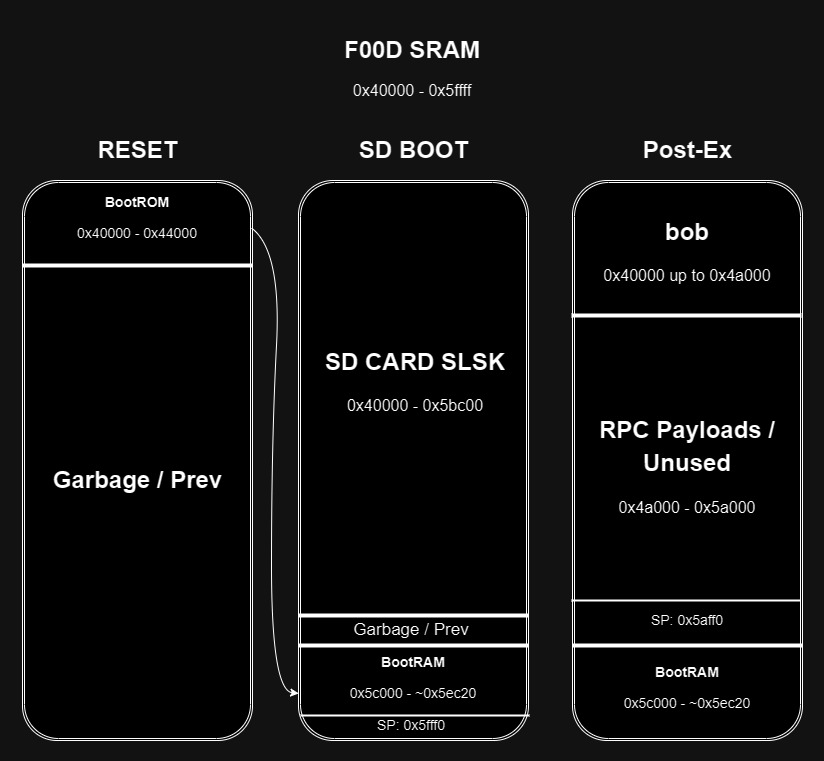
In sdboot, after copying itself from 0x40000 to 0x5c000, BootROM first reads a single block (0x200 bytes) from the external storage to 0x40000, verifies if second_loader offset and size fields are valid, then reads second_loader to 0x40000.
The issue is that the exception vectors are hardcoded to 0x40000, so any exceptions in BootROM during (or after) second_loader is read will cause a "jump" to the read data - resulting in arbitrary code execution.
Code execution
A simple way to trigger an exception is to perform a Fault Injection attack. Because all faults/exceptions result in code execution, the FI setup does not need to be precise, and can be approached in a spray-and-pray manner.
This project makes use of Voltage Fault Injection, specifically the "crowbar" method, performed by a low cost setup with the Teensy 4 mcu system at heart.
The result is a consistent BootROM code execution of a arbitrary code blob loaded from an unauthenticated MMC/SD storage inside the GameCard slot.
BootROM RPC
With psp2sdboot, the default code blob is bob, it starts an RPC server that can be used for research or executing additional specialized payloads with functionality such as key retrieval, data dumping, unbricking and more.
Supported units
- DEM-3000 : only IRT-002
- Due to an unknown JIG interface-enable procedure on IRT-001 / "slideys"
- CEM-3000 : supported
- PCH-1000 : supported
- VTE-1000 : supported
- PCH-2000 : not yet supported
- Due to lack of success triggering exceptions with Voltage Fault Injection
Setup
Requirements
- a working syscon JIG setup
- logic analyzer with at least two channels, a simple USB 8ch saleae/clone should work
- GC-SD adapter such as "sd2vita", with a micro/sd up to 2TiB
- consistent, configurable pulse generator that can set 1v+ for 100ns or less.
- for this project, the Teensy 4.0 / Teensy 4.1 mcu board was chosen for its high speed, tight-coupled memory and gpio controllers
- a chipwhisperer (lite) was also successfully used in this project's early iterations
- fast switching, logic level n-mosfet
- depending on your soldering skills/setup, a breakout board might be a good idea
- for this project, IRLML2502 and IRLML6246 were used
- 3.3v usb<->uart adapter for communicating with the Teensy 4 mcu board
Teensy
- Connect the Teensy 4 to a PC, enter bootloader mode
- Flash the latest build of teensy4vfi using Teensy Loader
- Connect the usb<->uart adapter
- PC TX -> Teensy pad 0 (RX)
- PC RX -> Teensy pad 1 (TX)
- GND
Solder points
There are at least two (magnet) wire solder points - Core_VDD (orange) and GC_dat0 (yellow).
- PCH-1000/PDEL-1000/CEM-3000/DEM-3000: front
- VTE-1000: front | back
- It is recommended to add a separate GND wire for the MOSFET.
Wiring
The MOSFET wires should be insulated and kept as short as possible, you can even solder its legs directly to the Core_VDD capacitor.
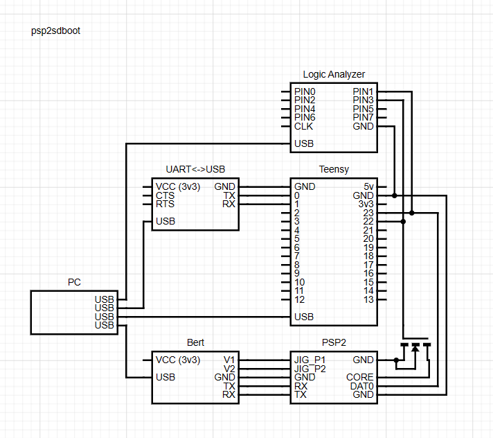
Software
The original setup was Windows + WSL1, but the instructions should work fine on Windows, Linux and MacOS.
Prerequisites
- Python 3.10+
- GCC
- Saleae Logic
- or whatever software your Logic Analyzer uses
- local copies of psp2sdboot, teensy4vfi, bob, and bert
- (optional) mepsdk
Environment
The "root", working directory should be a local copy of this repository.
- compile
tools/mkfake.c with GCC
- create symlinks for
bob/bob_rpc.py, teensy4vfi/teensy_rpc.py, and bert/bert.py
- create a
bob directory in payloads/, and copy there the bob build and header files
bob/build/* to payloads/bob/bob/source/include to payloads/bob/
- "set" the environment by running the provided
env.bat
- this simply sets a bunch of aliases
microSD card
A raw SD card image can be created using the previously compiled mkfake utility, the syntax is mkfake <code_blob> -o <output> where:
- code_blob is bob's glitch build -
payloads/bob/bob_glitch.bin
- output will be the SD card image
The prepared SD card must then be inserted in the target's GC slot.
SD Boot
The provided sdboot.py is a python script that loops reboot->glitch->check until bob is successfully loaded and executed.
Its accepted arguments/parameters and their descriptions can be listed with sdboot help.
Calibration
The first step is determining optimal timing parameters range for the main sdboot script, which will then find the more precise/consistent glitch timings.
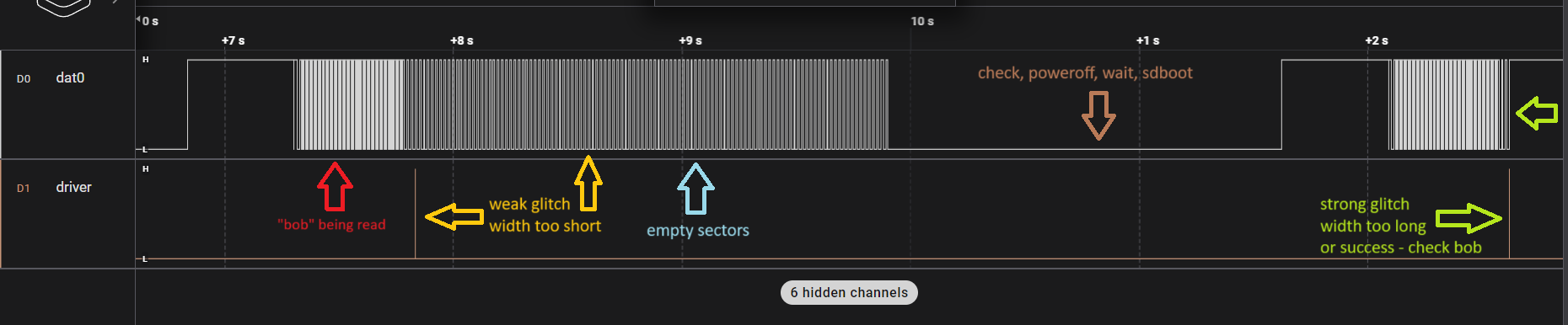
The "threshold" width
The width of a glitch that always causes an unrecoverable crash is called the "threshold", this should be the upper width boundary - sdboot's width_max argument.
It can be determined by the following procedure:
sdboot width=100 width_max=100000 width_step=100
- note the width at which dat0 cut off
- if there is no dat0 cut off until 100000, the setup is wrong/faulty
sdboot width=<cutoff_width-100> width_max=<cutoff_width+100> width_step=20
- repeat at least 5 times
- note the width at which dat0 always cuts off, this is the "threshold"
- If the "threshold" is below 200, it might indicate a faulty circuit, slow mosfet, or a very isolated/clean setup.
The "up_to_read" offset
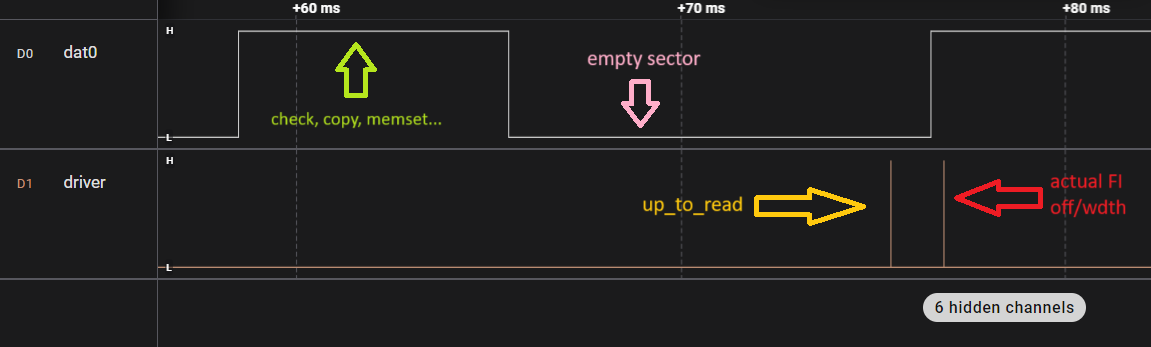
up_to_read is a special 0-width glitch queued to find an empty sector read op, which compensates for a high SD init/read jitter.
The idea is that as long as it lands in the middle of an empty sector being read (dat0 pulled down), the actual fault injection glitch can be precisely triggered and timed from dat0 going up.
It can be determined by altering the following command: sdboot up_to_read_mark=100 up_to_read=298400000. Change up_to_read until the mosfet line spike happens around the middle of an empty sector read.
Glitching
The second step is running the sdboot python script, and letting it find a correct combination of offset and width parameters
Script arguments are based on the values found during the Calibration step, with an added broad offset range:
sdboot up_to_read=<up_to_read> width=<threshold-(2*width_step)> width_max=<threshold+width_step> width_step=20 offset=100 offset_max=10000 offset_mult=10 offset_step=40
- offset* parameters should initially be broad, with further loops being more precise (eg offset_mult=1)
- if the threshold is below 500, width_step=10 might be a better choice
- if the starting width (threshold - (2 x width_step)) is observed to cut off dat0, the starting width should be decreased by width_step-sized decrements
- ultimately it depends on luck, it might take hours or even days to find a working offset and width pair
- in case of success, a
got sd boot: off=<offset>[<offset_mult>] width=<width> message will be displayed and the script will stop
Post-Exploitation
After bob presence is confirmed with bob ping, you can use the bob_rpc script to conduct further research or copy and run MeP payloads. Available RPC commands can be listed by calling the script without any arguments - bob.
RPC payloads
You should put your custom payloads inside the payloads/ directory.
They can statically link to bob and bootrom for basic funtionality, see the linker example. Headers can be found in payloads/bob/include/.
Payloads can be executed anywhere in the physical memory, keep in mind that some is uninitialized - eg DRAM.
- copy:
file_send <offset> <payload_file>
- exec:
exec <offset> <arg0> <arg1> <arg2_data>, where arg2_data is a buffer passed as arg2
- extended exec:
exece <offset> <arg0> <arg1> <arg2> <arg..>, up to 8 args total
Key extraction
Provided is a basic keydumper - payloads/keydumper - it can be used to get the SLSK enc/dec key partials, SNVS enc/dec keys, and the SMI encryption keys.
- If you do not have SoC TX wired, you can dump the key buffer from 0x1f850000 to a file using
bob file_dump.
Storage R/W
The provided eMMC dumper - payloads/emmc-dump - contains code to read/write eMMC as well as the SD card. It can be used for larger data handling, eMMC dump/unbrick, crypto research and more.
- By default, the emmc dumper uses DRAM which must be first initialized. Until reimplemented, the code/binary can be copied from second_loader.
- You can just use a different memory region, eg SPAD128K
Unbricking
At the time of writing, there is no single tool to diagnose and fix common "bricks".
You need to get the boot log, read henkaku wiki to find the probable brick cause, and use the provided tools/payloads to fix the console.
- SoC TX - for boot log - can be redirected to Syscon TX / USB TX by changing nvs byte 0x481 from 0xFF to 0x00,
nvs-write 0x481 0x1 00
- some more uncommon bricks might require you to reverse engineer the OS, i recommend Ghidra
Credits
This project was made in collaboration with Proxima and Mathieulh.
Additional thanks to:
- xyz - for help with hardware work, research, intial glitching, tests, spoonfeeding and handholding
- yifanlu and Team Molecule, whose work served as the foundation for this project
- all bert contributors
- henkaku wiki contributors


