2 layers407 × 184 mm
TRS-80-Model I G E1
RetroStack/TRS-80-Model-I-G-E1
Hardware Replica of the TRS-80 Model I Revision G
230 parts57MIT

 RetroStack/TRS-80-Model-I-Jap50-E11
Hardware Replica of the TRS-80 Model I Revision HE11E011550
TRS-80-Model I Jap50-E1 is an open-source printed circuit board by RetroStack, from the RetroStack/TRS-80-Model-I-Jap50-E1 repository on GitHub, published under the MIT licence. It is a 2-layer board of 407 × 184 mm with 253 parts on 410 nets, routed with 8,873 tracks and 739 vias.
It is built around the 74LS367PC, 74LS245SC and 74LS157PC, with the 74LS93SC, 74LS32SC and 74LS74PC among its other parts. Its parts include 78 resistors, 68 capacitors, 3 transistors, 3 connectors and 1 crystal.


This project is a faithful reimplementation of the mainboard of the iconic TRS-80 Model 1 (Revision HE11E011550) computer, redesigned and produced in Japan later in its existance. My own revision is designed to replicate the original system's functionality by using a PCB design 1-to-1 to the original, including components, interfaces, and even traces. The entire project is available under the MIT license.
WARNING: This project has not been confirmed to work yet. Use at your own risk.
<No photo available yet!>
NOTE: This board was reconstructed from photos and using an earlier board (Japanese-20 board) as reference. Therefore, the majority of traces are accurate, but a few (~18)might slightly deviate from the original design.
In the "Latest" folder, you'll find the most up-to-date design files, including:
The replica has been implemented using KiCAD 9. The KiCAD project files are included in this repository.
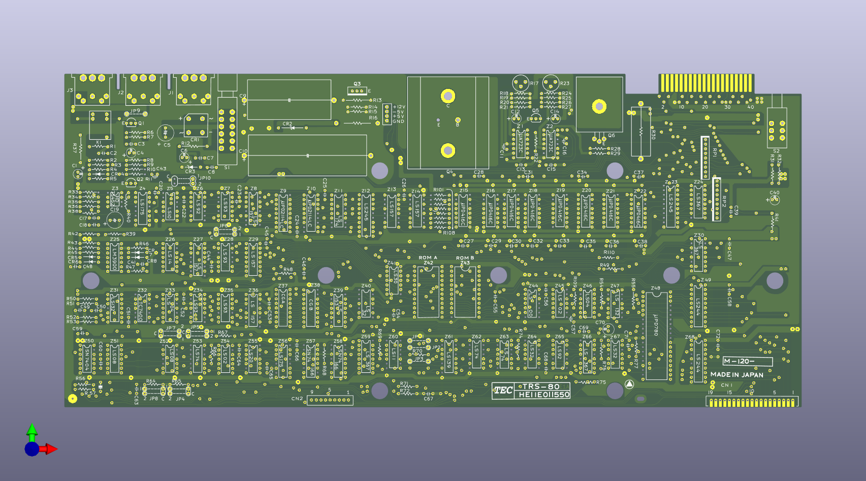
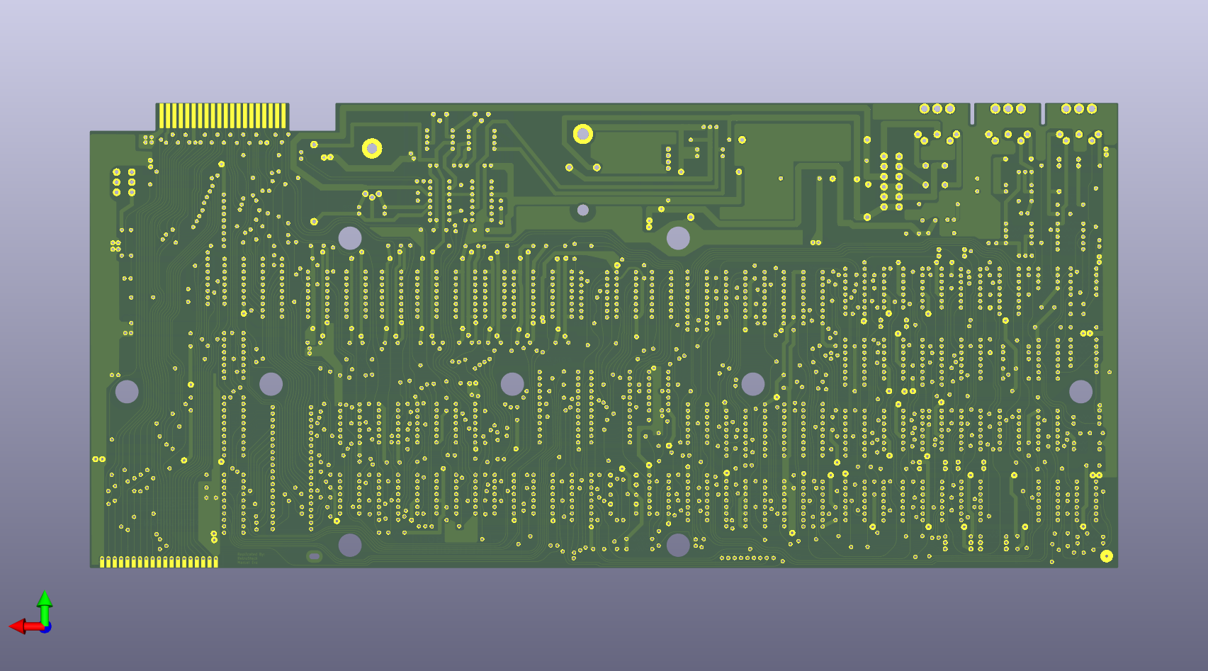
For each step, check if there is a connection between pad 1, 8, 9, 16 on Z18 (all four corners of the dynamic RAM IC). That IC needs all 3 voltages with ground. If any of them are shorted, then you know what you did most recently. Finding the cause of the short should then be relatively easy.
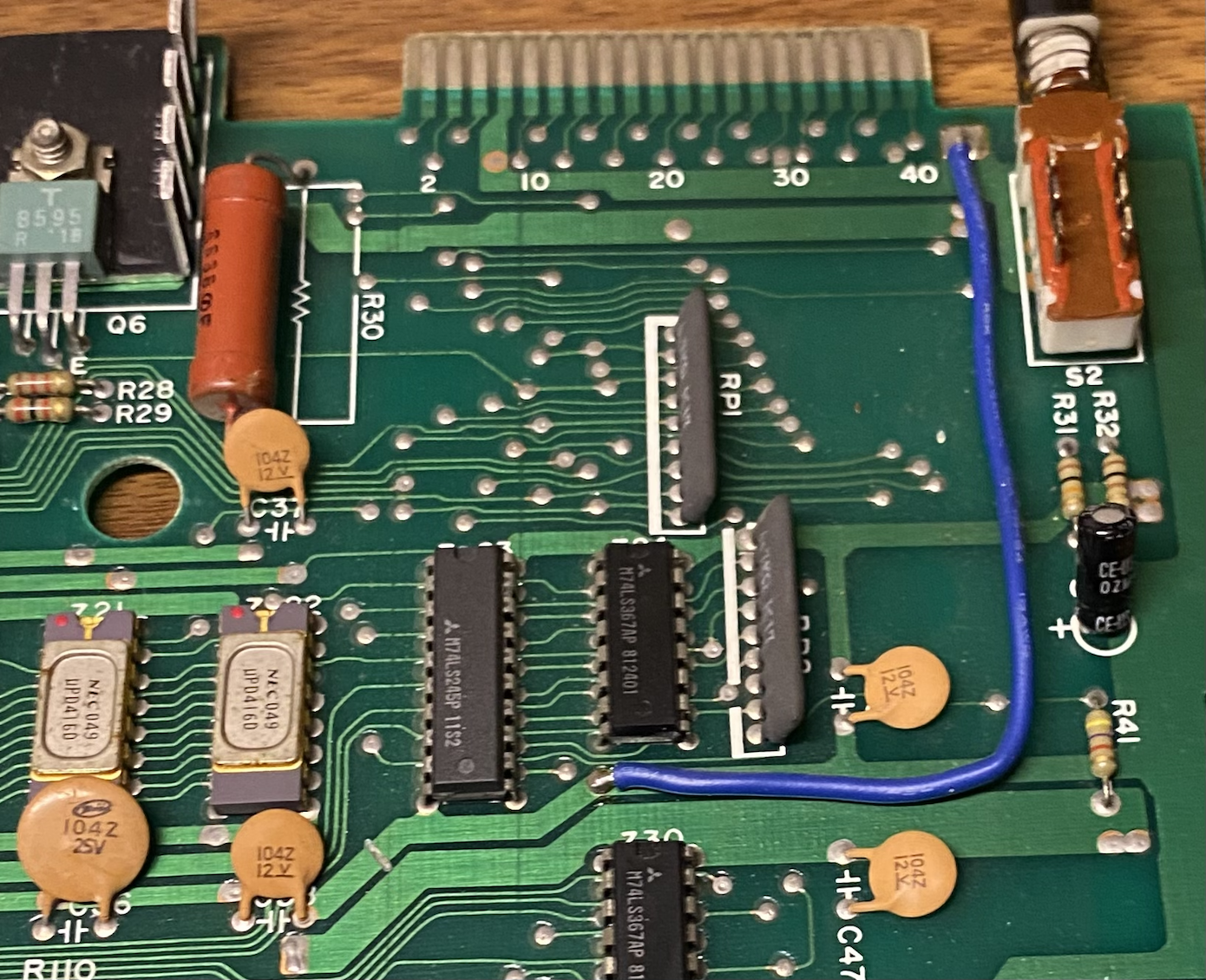
When ordering the board from a PCB manufacturer, you can select the following to get a more faithful version of the board:
Dimension: 407mm x 184mm
Layers: 2
Base Material: FR-4 TG 135-140 (and up)
PCB Thickness: 1.6mm
PCB Color: Green
Silkscreen Color: White
Via Covering: Untented
Surface Finish: Lead Free HASL
Outer Copper Weight: 1oz
Gold Fingers / Card Edge: yes (chamfer: 30 degrees)
Castellated Holes: no
Additionally, supply the following comment for the manufacturer:
Card edge is only on the upper right. The bottom right is just a connector and does not need to be chamfered.
There are some missing pads on the top layer. That is correct. Please leave them as-is.
This addresses recurring questions from some of the interesting design choices that were used on the original board which was replicated.
Below is a list of materials needed to assemble a complete system.
| Reference | Qty | Value | Component | Description | Comment |
|---|---|---|---|---|---|
| PCB | 1 | - | Replica Board | ||
| C1, C4, C6, C12, C14, C40 | 6 | 10uF 16V | C_Polarized | ||
| C2, C8, C20, C22, C23, C24, C25, C26, C28, C29, C31, C32, C34, C35, C37, C38, C39, C41, C44, C45, C46, C47, C49, C51, C52, C53, C54, C55, C56, C58, C59, C63, C64, C65, C66, C67, C68, C69, C71, C72 | 40 | 0.1uF 12V | Unpolarized capacitor | ||
| C3, C7, C13, C15 | 4 | 0.01uF 24V | Unpolarized capacitor | ||
| C5 | 1 | 220uF 16V | C_Polarized | ||
| C9 | 1 | 2200uF 35V | C_Polarized | ||
| C10 | 1 | 10000uF 16V | C_Polarized | ||
| C11, C16, C48, C57 | 4 | 1nF | Unpolarized capacitor | ||
| C17, C18 | 2 | 220pF | Unpolarized capacitor | ||
| C19 | 1 | 100uF 16V | C_Polarized | ||
| C27, C30, C33, C36 | 4 | 0.1uF 25V | Unpolarized capacitor | ||
| C43 | 1 | 100pF | Unpolarized capacitor | ||
| C50 | 1 | 2.7nF | Unpolarized capacitor | ||
| C60 | 1 | 47pF | Unpolarized capacitor | ||
| C70 | 1 | 22uF 16V | C_Polarized | ||
| CN1 | 1 | - | Generic connector, single row, 01x20 | Keyboard Connector | |
| CR1 | 1 | MDA202 | Bridge Rectifier | ||
| CR2 | 1 | 1N4735 | D_Zener | Zener diode | |
| CR3 | 1 | 1N5231 | D_Zener | Zener diode | |
| CR4, CR5, CR6, CR7, CR8 | 5 | 1N4148 | D | Diode | |
| J1, J2, J3 | 3 | Front View | DIN-5_180degree | 5-pin DIN connector (5-pin DIN-5 stereo) | |
| JP1, JP2, JP3, JP9 | 4 | - | Single Jumper | See description on Github or schematics | |
| JP4, JP5, JP6, JP7, JP8, JP10 | 6 | - | Double Jumper | See description on Github or schematics | |
| K1 | 1 | Relay_SPDT | Relay | Cassette Interface Relay | |
| Q1 | 1 | C1815 | NPN BJT Transistor | ||
| Q2, Q5 | 2 | A1015 | PNP BJT Transistor | ||
| Q3 | 1 | TIP29A | TIP29A | Q_NPN_BCE | |
| Q4 | 1 | 2N6594 | 2N6594 | Q_PNP_BEC | Replacement RS2040, MJ2955G |
| Q6 | 1 | MJE34 | MJE34 | Q_PNP_BCE | Replacement TIP32C |
| - | 1 | - | Heatsink | Q4 Heatsink | |
| - | 1 | - | Screw | M3x10mm | |
| - | 1 | - | Nut | M3 | |
| - | 1 | - | Heatsink | Q6 Heatsink | Smaller than original; no need to be big |
| - | 2 | - | Screw | M4x10mm | |
| - | 2 | - | Nut | M4 | |
| - | 1 | - | Thermal Grease | For Q4 and Q6 | Apply with Q-Tip or similar |
| R1, R32 | 2 | 100 | Resistor 0.25W (brown, black, brown, gold) | ||
| R2, R18, R19, R28 | 4 | 1.2k | Resistor 0.25W (brown, red, red, gold) | ||
| R3, R4 | 2 | 7.5k | Resistor 0.25W (violet, blue, red, gold) | ||
| R5 | 1 | 220k | Resistor 0.25W (red, red, yellow, gold) | ||
| R6 | 1 | 75 | Resistor 0.25W (violet, green, black, gold) | ||
| R7 | 1 | 47 | Resistor 0.25W (yellow, violet, black, gold) | ||
| R8, R75, R101, R102, R103, R104, R105, R106, R107, R108, R109, R110 | 12 | 330 | Resistor 0.25W (orange, orange, brown, gold) | ||
| R9 | 1 | 120 | Resistor 0.25W (brown, red, brown, gold) | ||
| R10 | 1 | 270 | Resistor 0.25W (red, violet, brown, gold) | ||
| R11, R31, R34, R49 | 4 | 10k | Resistor 0.25W (brown, black, orange, gold) | ||
| R12, R37 | 2 | 220 | Resistor 0.5W (red, red, brown, gold) | ||
| R13 | 1 | 68 | Resistor 0.25W (blue, grey, black, gold) | ||
| R14 | 1 | 2.7k | Resistor 0.25W (red, violet, red, gold) | ||
| R15 | 1 | 750 | Resistor 0.25W (violet, green, brown, gold) | ||
| R16 | 1 | 0.33 | Resistor 2W (orange, orange, silver, gold) | ||
| R17, R23 | 2 | 1k | Resistor 0.25W (brown, black, red, gold) | ||
| R20 | 1 | 100k | Resistor 0.25W (brown, black, yellow, gold) | ||
| R21, R24, R25 | 3 | 3.3k | Resistor 0.25W (orange, orange, red, gold) | ||
| R22 | 1 | 1.5k | Resistor 0.25W (brown, green, red, gold) | ||
| R26 | 1 | 2.2k | Resistor 0.25W (red, red, red, gold) | ||
| R27 | 1 | 12k | Resistor 0.25W (brown, red, orange, gold) | ||
| R29 | 1 | 2k | Resistor 0.25W (red, black, red, gold) | ||
| R30 | 1 | 5.6 | Resistor 3W (green, blue, gold, gold) | ||
| R33, R51 | 2 | 1M | Resistor 0.25W (brown, black, green, gold) | ||
| R35 | 1 | 680k | Resistor 0.25W (blue, grey, yellow, gold) | ||
| R36 | 1 | 1.8M | Resistor 0.25W (brown, grey, green, gold) | ||
| R38, R42 | 2 | 360k | Resistor 0.25W (orange, blue, yellow, gold) | ||
| R39 | 1 | 10 | Resistor 0.25W (brown, black, black, gold) | ||
| R40, R41, R48, R54, R55, R64, R65, R66, R67, R68, R69, R70, R71, R72, R74, R76, R77 | 17 | 4.7k | Resistor 0.25W (yellow, violet, red, gold) | ||
| R43 | 1 | 560k | Resistor 0.25W (green, blue, yellow, gold) | ||
| R44, R45, R46, R47, R50 | 5 | 470k | Resistor 0.25W (yellow, violet, yellow, gold) | ||
| R52, R53 | 2 | 8.2k | Resistor 0.25W (grey, red, red, gold) | ||
| R56, R57 | 2 | 910 | Resistor 0.25W (white, brown, brown, gold) | ||
| RP1, RP2 | 2 | 4.7k | 8 Resistor Network | 9-pin bussed Resistor network | |
| S1 | 1 | Power | SW_4PST | Black Cap | + red & black cap |
| S2 | 1 | Reset | SW_DPST | Red Cap | + red cap |
| Y1 | 1 | 10.6445 MHz | Crystal | Two pin crystal | 10.6MHz replacement |
| Z1, Z2 | 2 | LM723C | LM723C_1 | Linear Regulator (adjustable) | |
| Z3 | 1 | 75452 | 75452 | Dual-Peripheral Drivers for High-Current, High-Speed Switching | |
| Z4, Z56 | 2 | 74LS175 | 74LS175 | 4-bit D Flip-Flop, reset | |
| Z5 | 1 | 74LS10 | 74LS10 | Triple 3-input D | |
| Z6, Z65 | 2 | 74LS92 | 74LS92 | Divide by 12 counter | |
| Z7, Z28, Z34, Z35 | 4 | 74LS93 | 74LS93 | Divide by 2 & 8 counter | |
| Z8, Z13, Z14, Z27, Z29, Z36 | 6 | 74LS157 | 74LS157 | Quad 2 to 1 line Multiplexer | |
| Z9, Z10 | 2 | 2114 | 2114 | 1K Static RAM (SRAM 4-bit) | |
| Z11 | 1 | 74LS174 | 74LS174 | Hex D-type Flip-Flop, reset | |
| Z12, Z23 | 2 | 74LS245 | 74LS245 | Octal Bus Transceivers with 3-State Outputs | |
| Z15, Z16, Z17, Z18, Z19, Z20, Z21, Z22 | 8 | 4116 | 4116 | 16kBit x 1 Bit Dynamic RAM | |
| Z24, Z30, Z59, Z66 | 4 | 74LS367 | 74LS367_Split | Hex buffer 3-State outputs | |
| Z25 | 1 | LM3900 | LM3900 | Quad operational amplifier | |
| Z26 | 1 | 74LS14 | 74LS14 | Hex Schmitt-Trigger Inverters | |
| Z31, Z47 | 2 | 74LS132 | 74LS132 | Quad 2-input D Schmitt trigger | |
| Z32 | 1 | 74C00 | 7400 | Quad 2-input D gate | A 74HC04 or 74HCT04 will work in a pinch, but it will not be a nice stable picture. |
| Z33, Z46 | 2 | 74LS04 | 74LS04 | Hex Inverter | |
| Z37, Z38 | 2 | - | 18-Pin Socket | 18-Pin Machined Socket | One is optional |
| Z37, Z38 | 2 | MCM6670 | MCM6670P | 128 x 7 x 5 Character Generator | One is optional; Adapter needed; parts below |
| Z39 | 1 | 74LS153 | 74LS153 | Dual Multiplexer 4 to 1 | |
| Z40, Z64, Z67 | 3 | 74LS32 | 74LS32 | Quad 2-input OR | |
| Z41 | 1 | 74LS30 | 74LS30 | 8-input D | |
| Z42, Z43 | 2 | - | 24-Pin Socket | 24-Pin Machined Socket | |
| Z42 | 1 | 2364_20L | 2364_20L | 2364 64kBit (8kb x 8) PROM | Adapter needed; parts below |
| Z43 | 1 | 2332_20L_21L | 2332_20L_21L | 2332 32kBit (4kb x 8) PROM | Adapter needed; parts below |
| Z44 | 1 | 74LS00 | 74LS00 | Quad 2-input D gate | |
| Z45, Z54 | 2 | 74LS02 | 74LS02 | Quad 2-input NOR gate | |
| Z48 | 1 | Z80CPU | Z80 | Z80 CPU | |
| Z49, Z68 | 2 | 74LS244 | 74LS244 | Octal Buffers with 3-State Outputs | |
| Z50 | 1 | 7404 | 7404 | Hex Inverter | Used for clock. Make sure to use a 7404, not a 74LS04. If you do, you might have to add a capacitor to the circuit. |
| Z51, Z52 | 2 | 74LS08 | 74LS08 | Quad 2-input AND gate | |
| Z53, Z62, Z63 | 3 | 74LS74 | 74LS74 | Dual D Flip-flop, Set & Reset | |
| Z55 | 1 | 74LS20 | 74LS20 | Dual 4-input D | |
| Z57, Z58 | 2 | 74LS166 | 74LS166 | Shift Register 8-bit, parallel load | |
| Z60 | 1 | 74LS11 | 74LS11 | Triple 3-input AND | |
| Z61 | 1 | 74LS139 | 74LS139 | Dual 2-line to 4-line Decoder/Multiplexer | |
| - | 1 | - | Jumper Wires | Connecting traces | See documentation |
| - | 1 | - | Port Cover | DIN-5 Port Cover | |
| - | 1 | - | Keyboard Connector Kit | Cable and headers for Mainboard and Keyboard | Solder angled header inward towards Z76 |
| Z37, Z38 | 2 | PCB | Character Generator | Character Generator PCB (MCM7760/4) | One is optional. Assemble with components below; no solder jumper needed |
| Z37, Z38 | 2 | 4.7k | Network Resistor; 7-Pin | Pull-up resistors | One is optional. |
| Z37, Z38 | 2 | - | 40-Pin Header | Machined Header | One is optional. Cut to length to 9 pins (2x) |
| Z37, Z38 | 2 | - | 5-Pin DIP Switch | Character ROM selector | One is optional. Add in 10-14 pads |
| Z37, Z38 | 2 | - | ROM | CharGen 32rf | One is optional. |
| Z42, Z43 | 2 | PCB | System ROM | System ROM PCB (2364/2332) | Assemble with components below; no SMD or solder jumper needed |
| Z42, Z43 | 2 | 4.7k | Network Resistor; 4-Pin | Pull-up resistors | |
| Z42, Z43 | 1 | - | 40-Pin Header | Machined Header | Cut to length to 12 pins (3x + 1x from above) |
| Z42, Z43 | 1 | - | 3-Pin DIP Switch | System ROM A | Add in 13-15 pads; cut perforation on ROM B adapter |
| Z42, Z43 | 2 | - | ROMs | System ROM A (Z33) & ROM B (Z34) | |
| Z42, Z43 | 1 | - | 4-Wire Cable | Twisted | Solder 3 inner pads below and 1 outer pad (any of the 3); Repeat with same color on same pads on other adapter |
To work with this KiCAD project, you'll need the RetroStack libraries for KiCAD. Please follow this link to access and install these libraries.
A big thank you to Howard Bowe for donating the Japanese Model 1 (Jap-20), and to Leslie Ayling for providing detailed photographs of his original Jap-50 board. Their contributions made it possible to reverse engineer and create such a detailed and accurate replica.
For additional resources related to the TRS-80 Model 1, be sure to check out the central page for the TRS-80 Model 1 on RetroStack.
RetroStack is passionate about exploring and preserving the legacy of older computer systems. My work involves creating detailed documentation and videos to share the knowledge. I am also dedicated to reviving these classic systems by reimplementing them and offering replacement parts at no cost. If you're keen on supporting this unique project, I invite you to visit my Patreon page. Your support would be immensely valuable and greatly appreciated!
This project is licensed under the MIT License - see the LICENSE file for details.
| Qty | Value | Footprint | References |
|---|---|---|---|
| 40 | 0.1uF 12V | Library:TRS80_Model_I_C_Disc_9.5L_4W_6P_Jap | C2, C20, C22, C23, C24, C25, C26, C28, C29, C31, C32, C34, C35, C37, C38, C39 +24 |
| 17 | 4.7k | Library:TRS80_Model_I_R_0.25W_Jap | R40, R41, R48, R54, R55, R64, R65, R66, R67, R68, R69, R70, R71, R72, R74, R76 +1 |
| 12 | 330 | Library:TRS80_Model_I_R_0.25W_Jap | R8, R75, R101, R102, R103, R104, R105, R106, R107, R108, R109, R110 |
| 8 | DRAM_4116 | Library:TRS80_Model_I_DIP16_Jap | Z15, Z16, Z17, Z18, Z19, Z20, Z21, Z22 |
| 6 | 10uF 16V | Library:TRS80_Model_I_C_Pol_Radial_5D_2.5P_Jap | C1, C4, C6, C12, C14, C40 |
| 6 | 74LS157 | Library:TRS80_Model_I_DIP16_Jap | Z8, Z13, Z14, Z27, Z29, Z36 |
| 5 | 1N4148 | Library:TRS80_Model_I_D_Jap | CR4, CR5, CR6, CR7, CR8 |
| 5 | 470k | Library:TRS80_Model_I_R_0.25W_Jap | R44, R45, R46, R47, R50 |
| 4 | 0.01uF 24V | Library:TRS80_Model_I_C_Disc_9.5L_4W_6P_Jap | C3, C7, C13, C15 |
| 4 | 0.1uF 25V | Library:TRS80_Model_I_C_Disc_9.5L_4W_6P_Jap | C27, C30, C33, C36 |
| 4 | 1.2k | Library:TRS80_Model_I_R_0.25W_Jap | R2, R18, R19, R28 |
| 4 | 10k | Library:TRS80_Model_I_R_0.25W_Jap | R11, R31, R34, R49 |
| 4 | 74LS367 | Library:TRS80_Model_I_DIP16_Jap | Z24, Z30, Z59, Z66 |
| 4 | 74LS93 | Library:TRS80_Model_I_DIP14_Jap | Z7, Z28, Z34, Z35 |
| 4 | TRS80_Model_I_Jumper_2_Jap | Library:TRS80_Model_I_Jumper_2_Open_Jap | JP1, JP2, JP3, JP9 |
| 3 | 1nF | Library:TRS80_Model_I_C_Disc_9.5L_4W_6P_Small_Jap | C11, C16, C57 |
| 3 | 3.3k | Library:TRS80_Model_I_R_0.25W_Jap | R21, R24, R25 |
| 3 | 74LS32 | Library:TRS80_Model_I_DIP14_Jap | Z40, Z64, Z67 |
| 3 | 74LS74 | Library:TRS80_Model_I_DIP14_Jap | Z53, Z62, Z63 |
| 3 | Front View | Library:TRS80_Model_I_DIN5_Jap | J1, J2, J3 |
| 2 | 100 | Library:TRS80_Model_I_R_0.25W_Jap | R1, R32 |
| 2 | 1M | Library:TRS80_Model_I_R_0.25W_Jap | R33, R51 |
| 2 | 1k | Library:TRS80_Model_I_R_Pot_Jap | R17, R23 |
| 2 | 220 | Library:TRS80_Model_I_R_0.5W_Jap | R12, R37 |
| 2 | 220pF | Library:TRS80_Model_I_C_Disc_9.5L_4W_6P_Jap | C17, C18 |
| 2 | 360k | Library:TRS80_Model_I_R_0.25W_Jap | R38, R42 |
| 2 | 4.7k | Library:TRS80_Model_I_R_Array_09_Jap | RP1, RP2 |
| 2 | 7.5k | Library:TRS80_Model_I_R_0.25W_Jap | R3, R4 |
| 2 | 74LS02 | Library:TRS80_Model_I_DIP14_Jap | Z45, Z54 |
| 2 | 74LS04 | Library:TRS80_Model_I_DIP14_Jap | Z33, Z46 |
| 2 | 74LS08 | Library:TRS80_Model_I_DIP14_Jap | Z51, Z52 |
| 2 | 74LS132 | Library:TRS80_Model_I_DIP14_Jap | Z31, Z47 |
| 2 | 74LS166 | Library:TRS80_Model_I_DIP16_Jap | Z57, Z58 |
| 2 | 74LS175 | Library:TRS80_Model_I_DIP16_Jap | Z4, Z56 |
| 2 | 74LS244 | Library:TRS80_Model_I_DIP20_Jap | Z49, Z68 |
| 2 | 74LS245 | Library:TRS80_Model_I_DIP20_Jap | Z12, Z23 |
| 2 | 74LS92 | Library:TRS80_Model_I_DIP14_Jap | Z6, Z65 |
| 2 | 8.2k | Library:TRS80_Model_I_R_0.25W_Jap | R52, R53 |
| 2 | 910 | Library:TRS80_Model_I_R_0.25W_Jap | R56, R57 |
| 2 | A1015 | Library:TRS80_Model_I_Q_Circle_ECB_Jap | Q2, Q5 |
| 2 | LM723C | Library:TRS80_Model_I_DIP14_Jap | Z1, Z2 |
| 2 | MCM6670 | Library:TRS80_Model_I_DIP18_Jap | Z37, Z38 |
| 2 | SRAM_2114 | Library:TRS80_Model_I_DIP18_Jap | Z9, Z10 |
| 2 | TRS80_Model_I_Jumper_3_Jap | Library:TRS80_Model_I_Jumper_3_Open_Jap | JP4, JP8 |
| 2 | TRS80_Model_I_Jumper_3_Jap | Library:TRS80_Model_I_Jumper_3_Open_HFlipped_VFlipped_Jap | JP6, JP7 |
| 1 | 0.33 | Library:TRS80_Model_I_R_2W_Jap | R16 |
| 1 | 1.5k | Library:TRS80_Model_I_R_0.25W_Jap | R22 |
| 1 | 1.8M | Library:TRS80_Model_I_R_0.25W_Jap | R36 |
| 1 | 10 | Library:TRS80_Model_I_R_0.25W_Jap | R39 |
| 1 | 10.6445 MHz | Library:TRS80_Model_I_Crystal_Jap | Y1 |
| 1 | 10000uF 16V | Library:TRS80_Model_I_C_Pol_Axial_63L_25W_71P_Jap | C10 |
| 1 | 100k | Library:TRS80_Model_I_R_0.25W_Jap | R20 |
| 1 | 100pF | Library:TRS80_Model_I_C_Disc_9.5L_4W_6P_Small_Jap | C43 |
| 1 | 100uF 16V | Library:TRS80_Model_I_C_Pol_Radial_10D_5P_Jap | C19 |
| 1 | 120 | Library:TRS80_Model_I_R_0.25W_Jap | R9 |
| 1 | 12k | Library:TRS80_Model_I_R_0.25W_Jap | R27 |
| 1 | 1N4735 | Library:TRS80_Model_I_D_Zener_Long_Jap | CR2 |
| 1 | 1N5231 | Library:TRS80_Model_I_D_Zener_Jap | CR3 |
| 1 | 1nF | Library:TRS80_Model_I_C_Disc_9.5L_4W_6P_Jap | C48 |
| 1 | 2.2k | Library:TRS80_Model_I_R_0.25W_Jap | R26 |
| 1 | 2.7k | Library:TRS80_Model_I_R_0.25W_Jap | R14 |
| 1 | 2.7nF | Library:TRS80_Model_I_C_Disc_9.5L_4W_6P_Jap | C50 |
| 1 | 2200uF 35V | Library:TRS80_Model_I_C_Pol_Axial_41L_19W_48P_Jap | C9 |
| 1 | 220k | Library:TRS80_Model_I_R_0.25W_Jap | R5 |
| 1 | 220uF 16V | Library:TRS80_Model_I_C_Pol_Radial_10D_5P_Jap | C5 |
| 1 | 22uF 16V | Library:TRS80_Model_I_C_Pol_Radial_5D_2.5P_Jap | C70 |
| 1 | 2332_20L_21L | Library:TRS80_Model_I_DIP24_Jap | Z43 |
| 1 | 2364_20L | Library:TRS80_Model_I_DIP24_Jap | Z42 |
| 1 | 270 | Library:TRS80_Model_I_R_0.25W_Jap | R10 |
| 1 | 2N6594 | Library:TRS80_Model_I_Q_Heatsink_Large_BEC_Jap | Q4 |
| 1 | 2k | Library:TRS80_Model_I_R_0.25W_Jap | R29 |
| 1 | 47 | Library:TRS80_Model_I_R_0.25W_Jap | R7 |
| 1 | 47pF | Library:TRS80_Model_I_C_Disc_9.5L_4W_6P_Jap | C60 |
| 1 | 5.6 | Library:TRS80_Model_I_R_3W_Jap | R30 |
| 1 | 560k | Library:TRS80_Model_I_R_0.25W_Jap | R43 |
| 1 | 68 | Library:TRS80_Model_I_R_0.5W_Jap | R13 |
| 1 | 680k | Library:TRS80_Model_I_R_0.25W_Jap | R35 |
| 1 | 7404 | Library:TRS80_Model_I_DIP14_Jap | Z50 |
| 1 | 74C00 | Library:TRS80_Model_I_DIP14_Jap | Z32 |
| 1 | 74LS00 | Library:TRS80_Model_I_DIP14_Jap | Z44 |
The 227 most common of 253 parts.
RetroStack/TRS-80-Model-I-G-E1
Hardware Replica of the TRS-80 Model I Revision G

RetroStack/TRS-80-Model-I-Expansion-Interface-Rev-D
Hardware Replica of the TRS-80 Model I Expansion Interface - Revision D


misterblack1/zenith_zt1
Information gathered on the Zenith ZT-1 / ZT-10 / ZT-11 and ZTX/ZT-x-A variants

RichCini/LomasBoards
Small repository of files/data related to Lomas Data Products S-100 boards.


clemarfolly/Microdigital-TK2000
Reprodução da PCB do TK-2000 da Microdigital, clone do Micro-Professor MPF-II

It measures 407 × 184 mm and has 2 copper layers, 1.6 mm thick.
253 parts, built around the 74LS367PC, 74LS245SC, 74LS157PC and 74LS93SC. The full list of its parts is on this page, with links to each part's symbol and footprint where PCBKit's library has them.
From the RetroStack/TRS-80-Model-I-Jap50-E1 repository on GitHub, at the commit this page was made from: the board is KiCAD/TRS80_Model_I_Jap50_E1.kicad_pcb and its schematic KiCAD/AddressDecoder.kicad_sch. PCBKit opens the board in the browser, with nothing to install.
Its repository publishes it under the MIT licence: you may reuse it on that licence's terms (keep the author's notice, and for a copyleft licence share your changes alike).