
2 layers88.9 × 50.8 mm
PCB Business Card
AmirAlsad/beta-rush-pcb-cards
NFC + silkscreen PCB cards designed for MIT Beta Theta Pi rush week 2025 — KiCad sources, vendored library, and as-manufactured gerbers.
11 parts

 Raziz1/PCB_Business_Card61
A PCB business card with NFC capabilities designed in KiCad
PCB Business Card is an open-source printed circuit board by Raziz1, from the Raziz1/PCB_Business_Card repository on GitHub. It is a 2-layer board of 88.9 × 50.8 mm with 9 parts on 7 nets, routed with 12 tracks and 0 vias.
It is built around the NT3H1101W0FTTJ. Its parts include 2 capacitors, 1 resistor, 1 IC and 1 diode. It belongs with the radio and wireless boards of this library.
The following project is a PCB designed as a business card. This card contains an integrated NFC tag that allows you to share your contact information wirelessly.
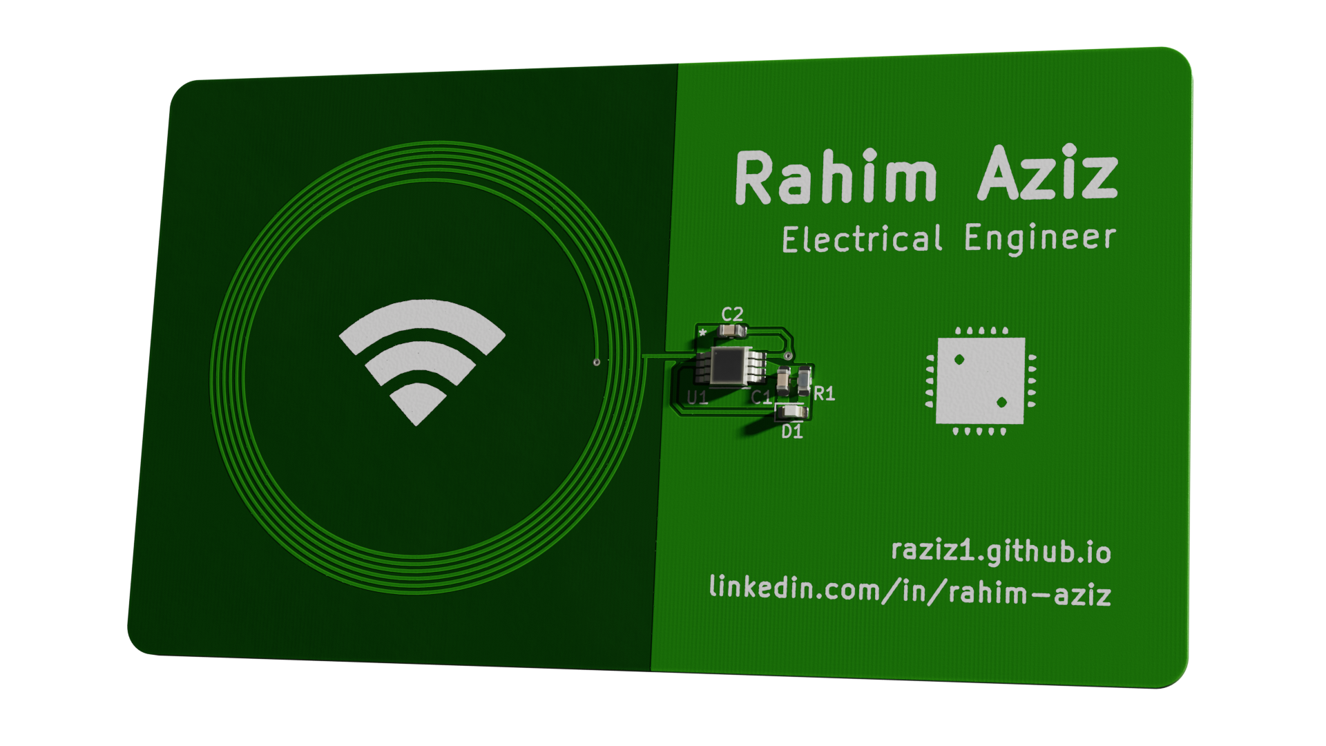
Blender Render
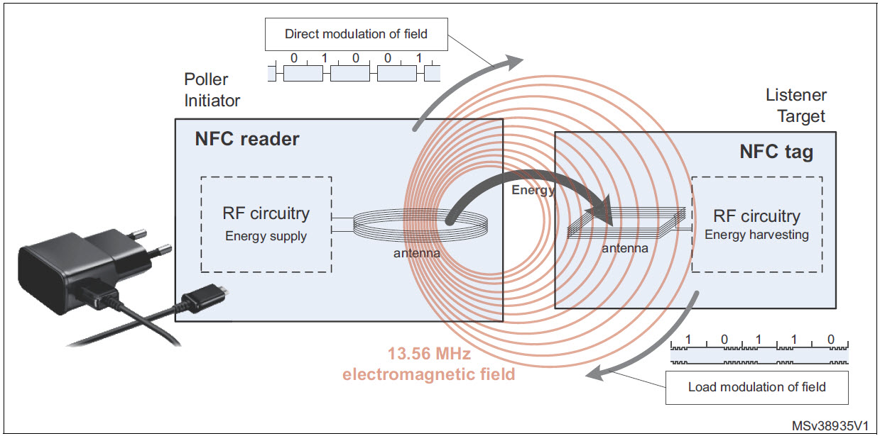
NFC (Near Field Communication) is a group of communication protocols that allows for low speed wireless communication between two electronic devices.
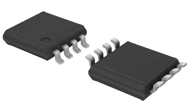
THe NFC IC being used in this project is the NT3H1101W0FTTJ.
The internet has a plethora of resources for antenna design. The two sources I will be referring to for this design are:
The figure below shows the equivalent electrical circuits of the dynamic NFC tag and its antenna.
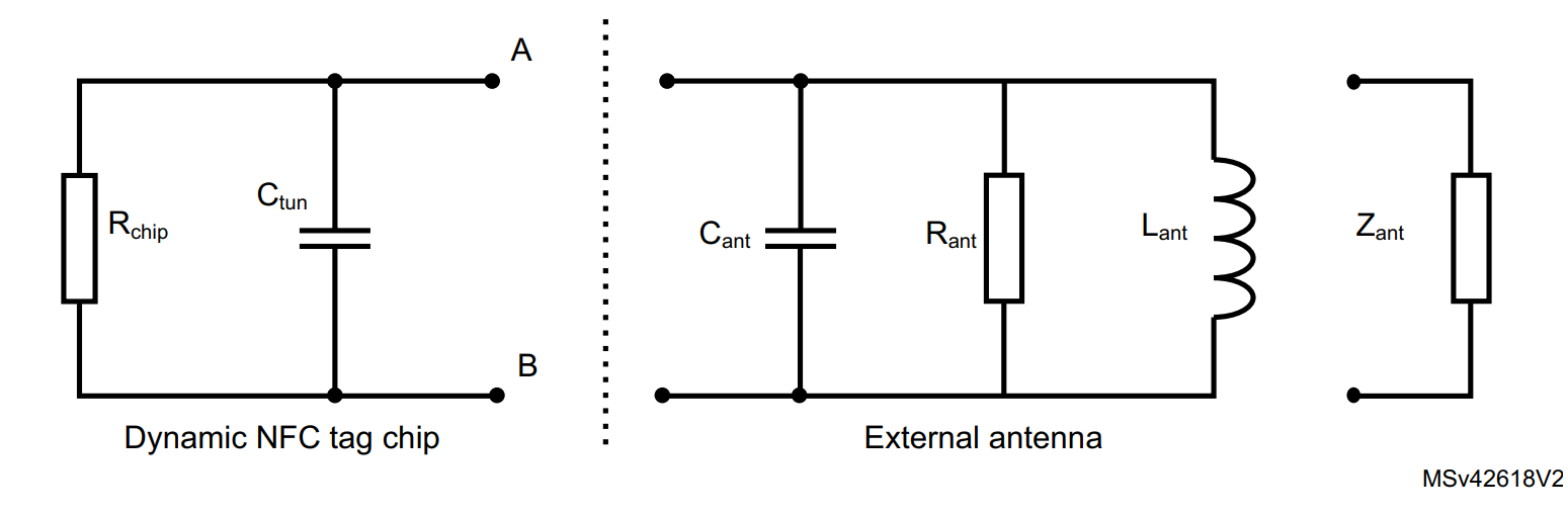
The above circuit can be simplified into an equivalent RLC circuit.
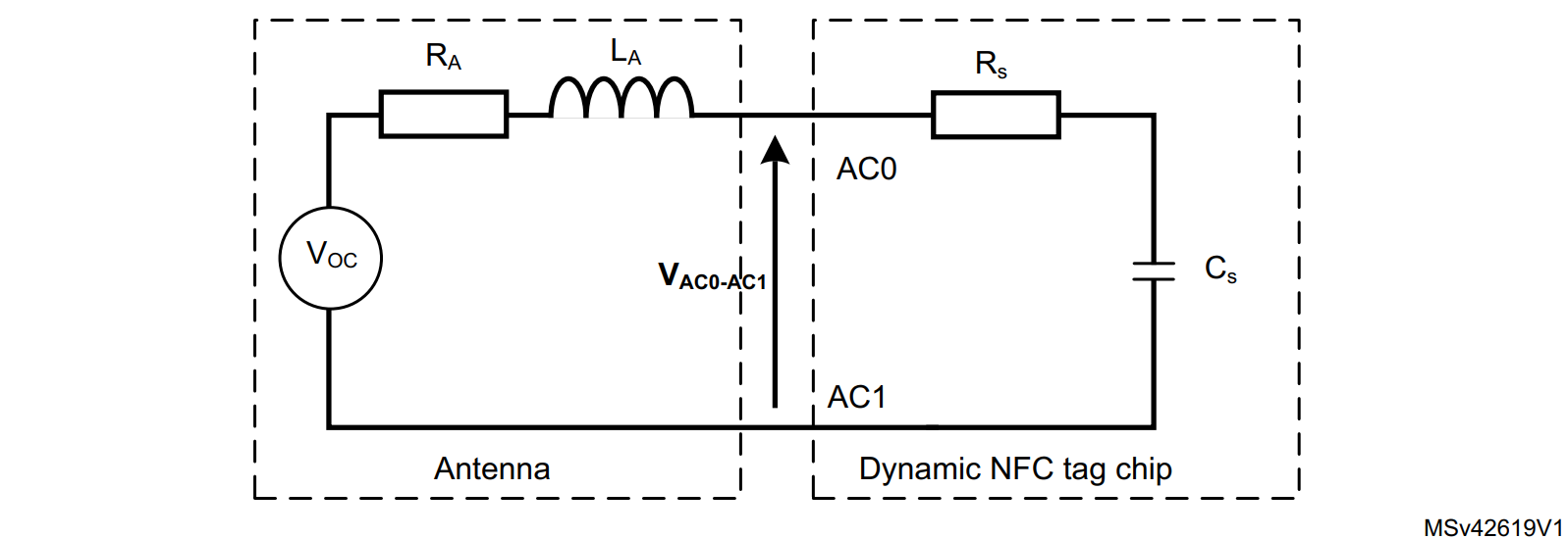
Based on the simplified RLC circuit we can determine the resonant frequency.
We know that for an NFC tag, the desired frequency is 13.56 MHz. We also know that the IC's parallel capacitance is 50 pF (from the datasheet). Ignore the parasitic capacitance of the antenna for now; we will come back to that. Based on this information, we can work backwards to determine the required inductance of the antenna.
$f_R=\frac{1}{2\cdot \pi \cdot \sqrt{L_{pc}\cdot C_{pl}}}$
$L_{pc}=\frac{1}{C_{pl}\left(2\pi f_R\right)^2}$
$L_{pc}=\frac{1}{5\cdot 10^{-11}\left(2\pi \cdot 13560000\right)^2} = 0.00000275518$
$L_{pc}=0.00000275518:H=:2.75518:uH$
We can now design an NFC antenna based on the desired inductance calculated above. To design the antenna I referred to various resources to confirm my calculations.
The AN11276 NTAG Antenna Design Guide provides the following information to design an antenna.
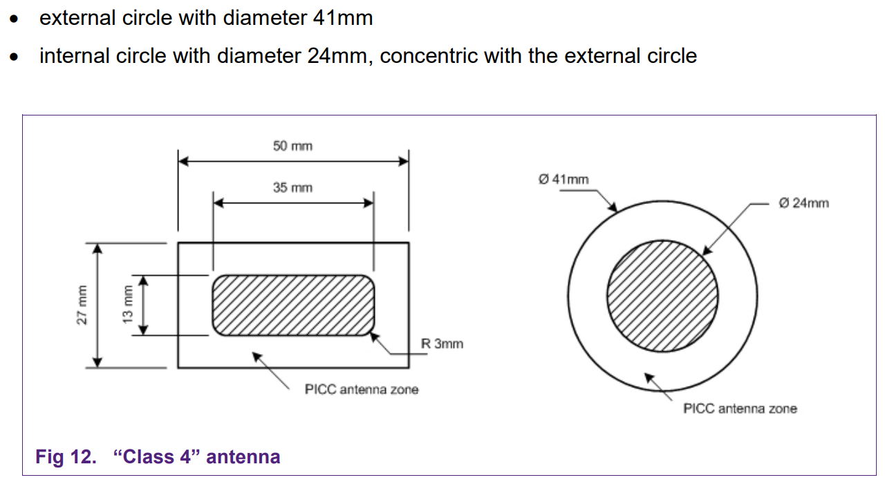
NXP Class 4 Antenna Design Recommendation
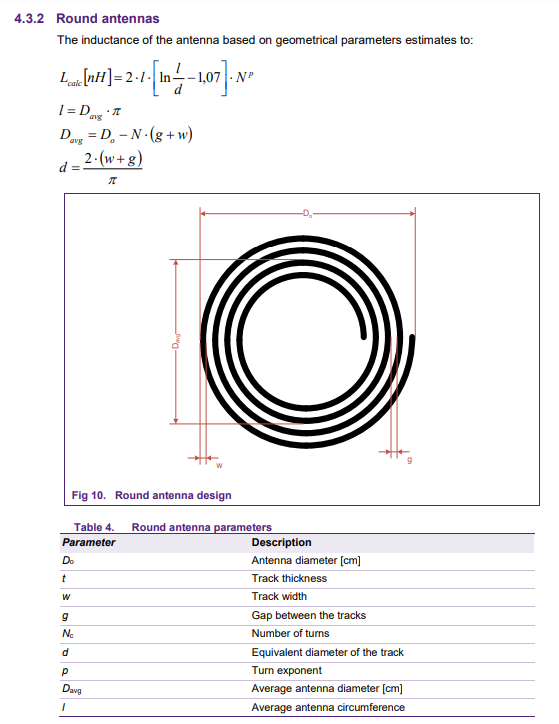
NXP Round Antennas Formula
I utilized the Antenna_Shape_Calculator excel document to calculate the geometric parameters. They were as follows:
The AN2972 Application note provides the following information to design an antenna.
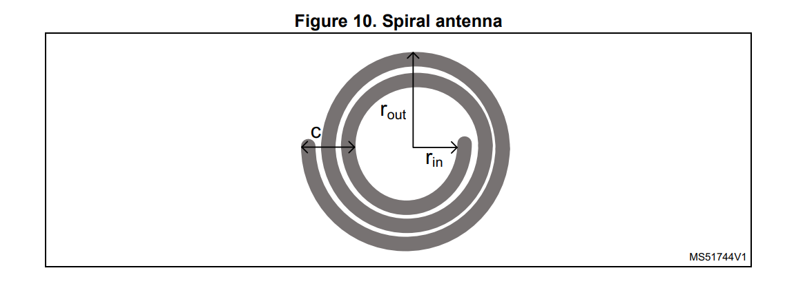
STM Spiral Antenna Design
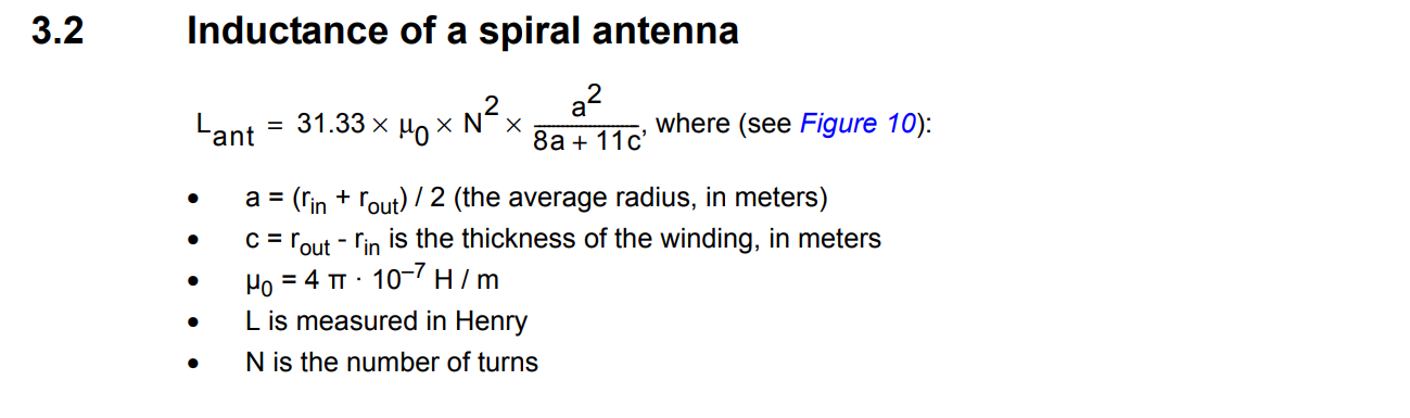
STM Spiral Antennas Formula
I utilized the Antenna_Shape_Calculator excel document to calculate the geometric parameters. They were as follows:
We are not quite ready to complete the design. Looking back at the equivalent circuit, we are still missing a few parameters: antenna capacitance, antenna resistance, and the NFC IC resistance. Typically, these parameters are determined by measuring the actual physical circuit design. For a guide on how to measure these parameters, check out the following link: --> Guide to designing antennas for the NTAG I2C plus. Nevertheless, we can make some rough estimations by utilizing various tools.
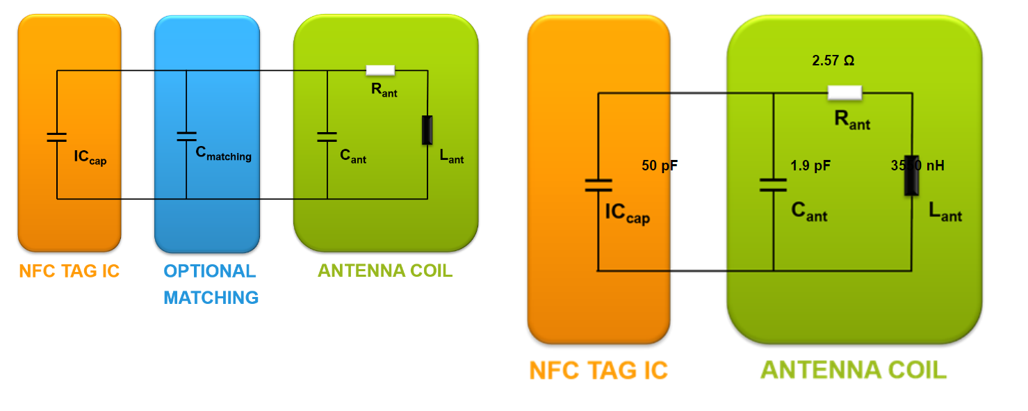
NXP NFC Antenna Tool
We can now work our way backwards to verify the parameters we calculated above. By rebuilding the equivalent circuit with these parameters in LTSpice, we can verify the resonance frequency. According to the simulation below, the resonance frequency is 13.35 MHz. This should be adequate for NFC; alternatively, we can target an inductance of 2.5-2.6 uH to achieve a resonance frequency that is closer to 13.56 MHz. Furthermore, an optional tuning capacitor can be added to get closer to 13.56 MHz.
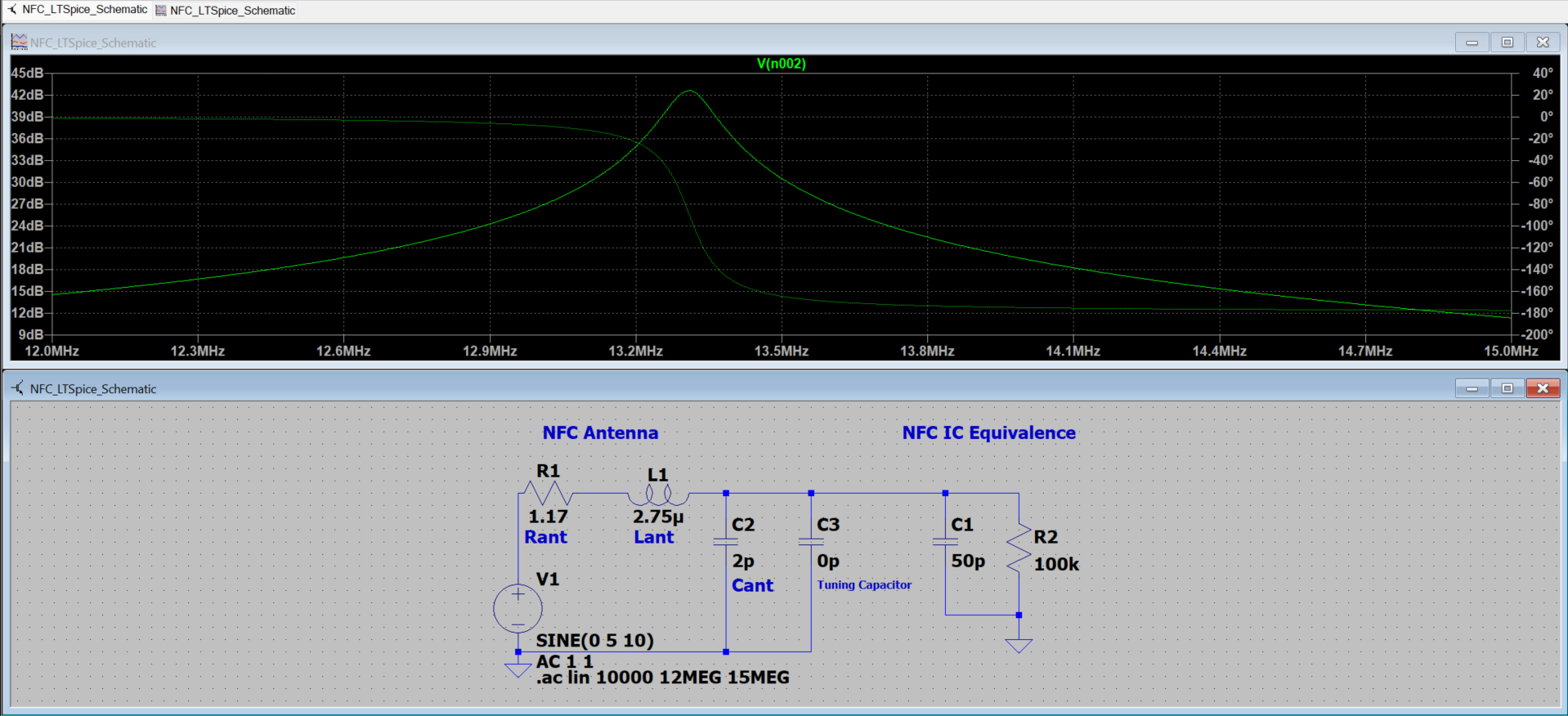
LTSpice Simulation
I decided to rerun the simulation and redesign the antenna parameters ($D_0 = 39mm$) to target an inductance of 2.576uH. This gives us more headroom to account for any imperfections in the manufacturing process. This allows us to use a tuning capacitor to bring the resonance frequency down and closer to 13.56 MHz.
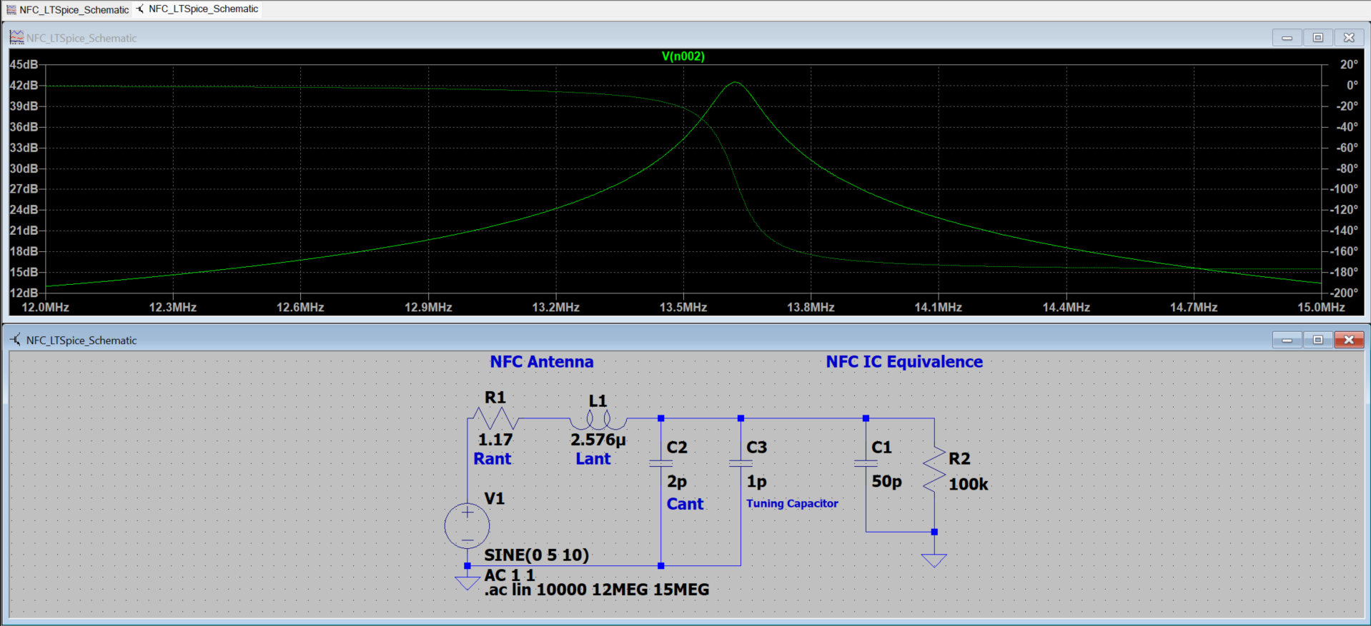
LTSpice Simulation with Tuning Capacitor
Antennas are typically simulated using electromagnetic simulation software to predict and optimize their real-world performance. A variety of tools are available, such as:
For this design, I chose to work with MATLAB’s Antenna Toolbox and RF Toolbox, as I did not yet have the experience to effectively use industry-grade tools like HFSS or CST.
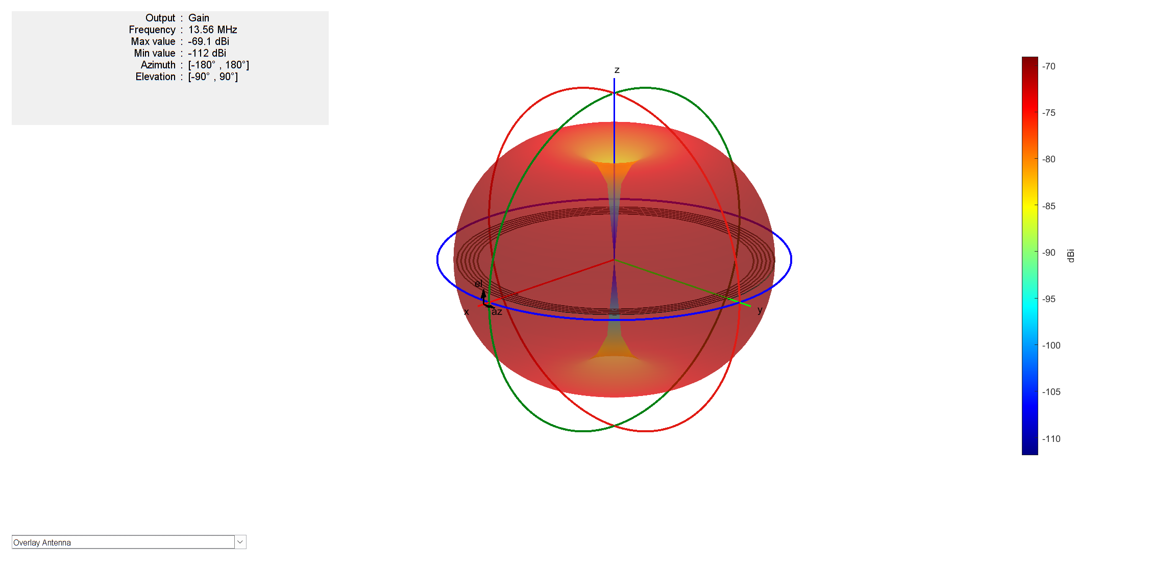
MATLAB 3D Radiation Pattern
After spending several days experimenting with the MATLAB script from the repository, I was unsuccessful in reproducing a clear resonance at 13.56 MHz. I tried designing the antenna directly in the Antenna Toolbox, carefully defining spiral coil parameters, trace width, spacing, and substrate properties. I also attempted to import the PCB layout into the PCB Antenna Toolbox using the gerber files of the actual NFC coil. Despite these efforts, the desired resonance could not be achieved. Following a discussion with Umar on the MATLAB Answers forum, it was clarified that the limitation lies in the software itself for this specific application:
- "MATLAB’s Antenna Toolbox is designed for far-field radiation analysis, not near-field inductive coupling. NFC, however, operates in the reactive near-field, where antennas behave as coupled inductors rather than radiating elements. The S11 parameters calculated in MATLAB inherently assume radiation losses, which do not accurately represent NFC coil physics." *
At this stage, Umar provided a toolbox-free MATLAB script that verified the design using RF first principles, which is available in the repository. The script addressed the following calculations:
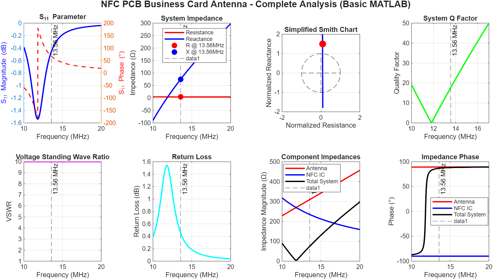
Umar Script Output
For the final design of the antenna I ended up settling on the following parameters:
For the schematic, I borrowed the idea of an LED indicator for the energy harvesting circuit from the PCB Business Card With NFC. The capacitor is to guarantee operation during RF communication. The resistor value was chosen to limit the current going through the LED. The value was determined by using the following equation:
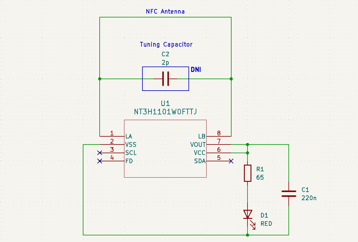
Schematic Design
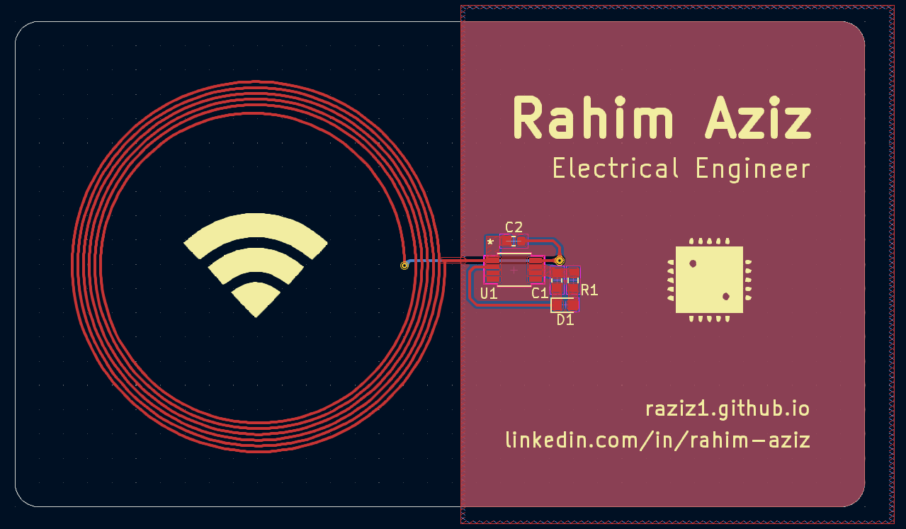
PCB Design
I ordered the board through PCBWay by using the KiCAD plugin. I assembled and soldered the components on the board myself.
For the PCBWay specification selection I chose the following options:
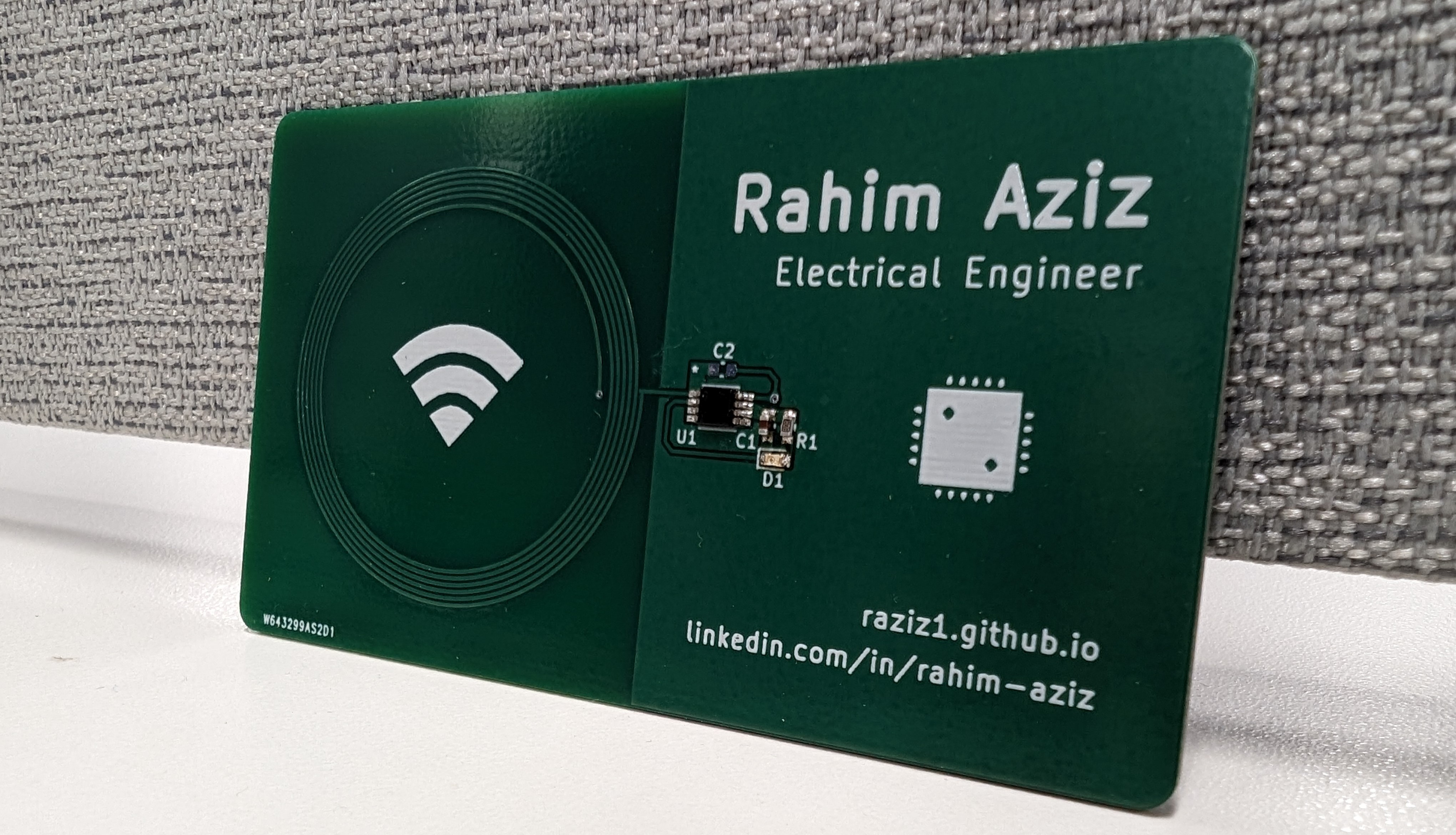
Final Product
Lastly, I programed the IC through the NFC TagWriter by NXP app.
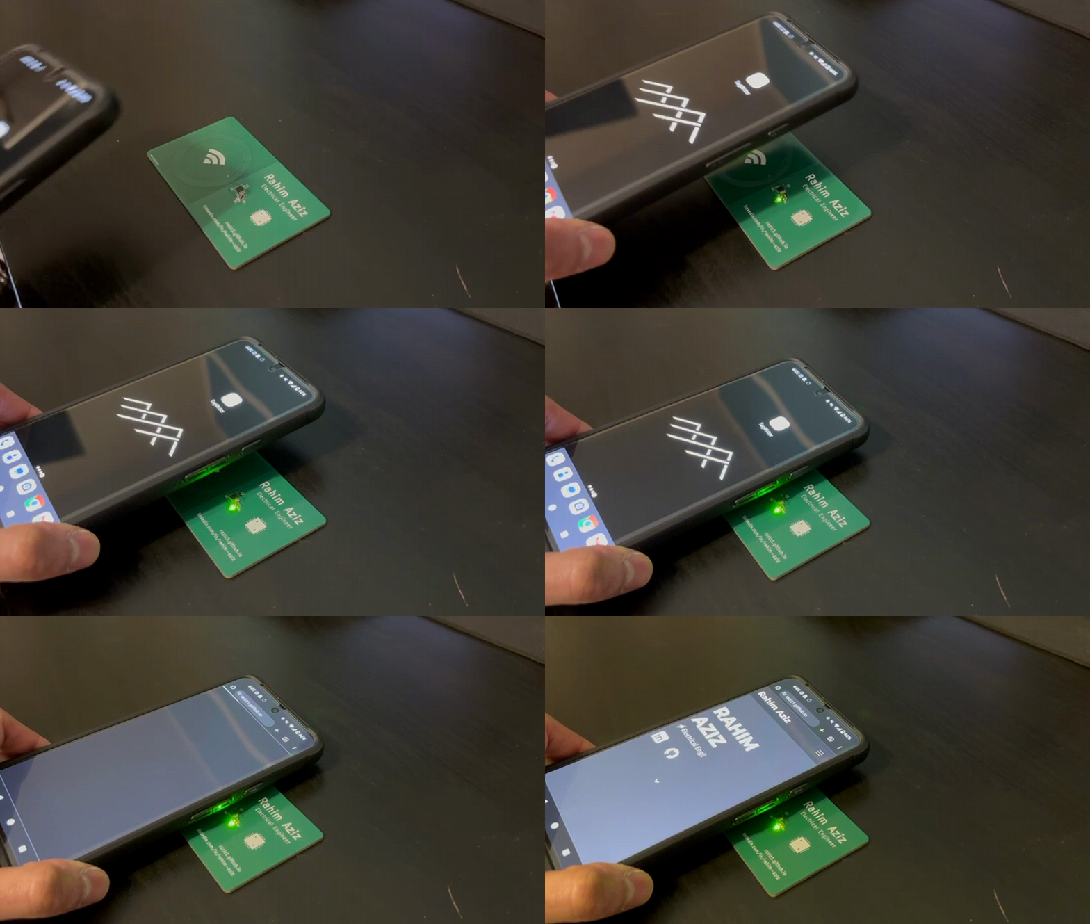
PCB in Action!
[!CAUTION]
iPhone Compatibility & Energy Harvesting Limit
During real-world testing, this card worked reliably on Android devices but failed to trigger background NFC reading on iPhones.
- Polling Fields: iPhones emit low-energy, brief polling bursts to conserve battery, whereas many Android phones broadcast significantly stronger, higher-energy continuous RF fields.
- Energy Starvation: When attempting to harvest energy from an iPhone, the on-board LED circuit drew too much current. This collapsed the harvested voltage rail before the NT3H1101’s digital core could boot and complete its initial communication handshake.
Circuit Current Consumption
Based on the populated components ($R = 64.9\ \Omega$ and a green LED with $V_f \approx 2.0\text{ V}$), the branch demands:
$$I_{LED} = \frac{V_{OUT} - V_{LED}}{R} = \frac{3.3\text{ V} - 2.0\text{ V}}{64.9\ \Omega} \approx 20\text{ mA}$$
Datasheet Limit
According to the NXP NT3H1101/1201 datasheet:
"The voltage and current from the energy harvesting depend on various parameters, such as the strength of the RF field, the tag antenna size, or the distance from the NFC device. At room temperature, NTAG I2C could provide typically 5 mA at 2 V on the VOUT pin with an NFC Phone.
Operating NTAG I2C in energy harvesting mode requires a number of precautions:
- A significant capacitor is needed to guarantee operation during RF communication. The total capacitor between VOUT and GND shall be in the range of 150nF to 200 nF.
Note that increasing the output current on the Vout decreases the RF communication range."
Because the IC typically delivers only up to 5 mA at 2 V under smartphone coupling, an active load demanding ~20 mA collapses the harvested rail on lower-power emitters like iPhones.
Fix: Leaving the LED/resistor unpopulated (or increasing the resistor to $\ge 1\text{--}2\text{ k}\Omega$ to limit current below $1\text{ mA}$) immediately restores instant background read compatibility on iPhones.
Finally, I wanted to characterize the response of the circuit using my Analog Discovery 2 - USB oscilloscope. In particular, I aimed to characterize and visualize the difference in responses when the circuit had and didn't have a tuning capacitor.
The first order of business was to utilize the network analyzer feature on the Analog Discovery 2. By attaching the wave generator on one end of the antenna and probing on the other we could sweep through various frequencies and observe the circuits response.
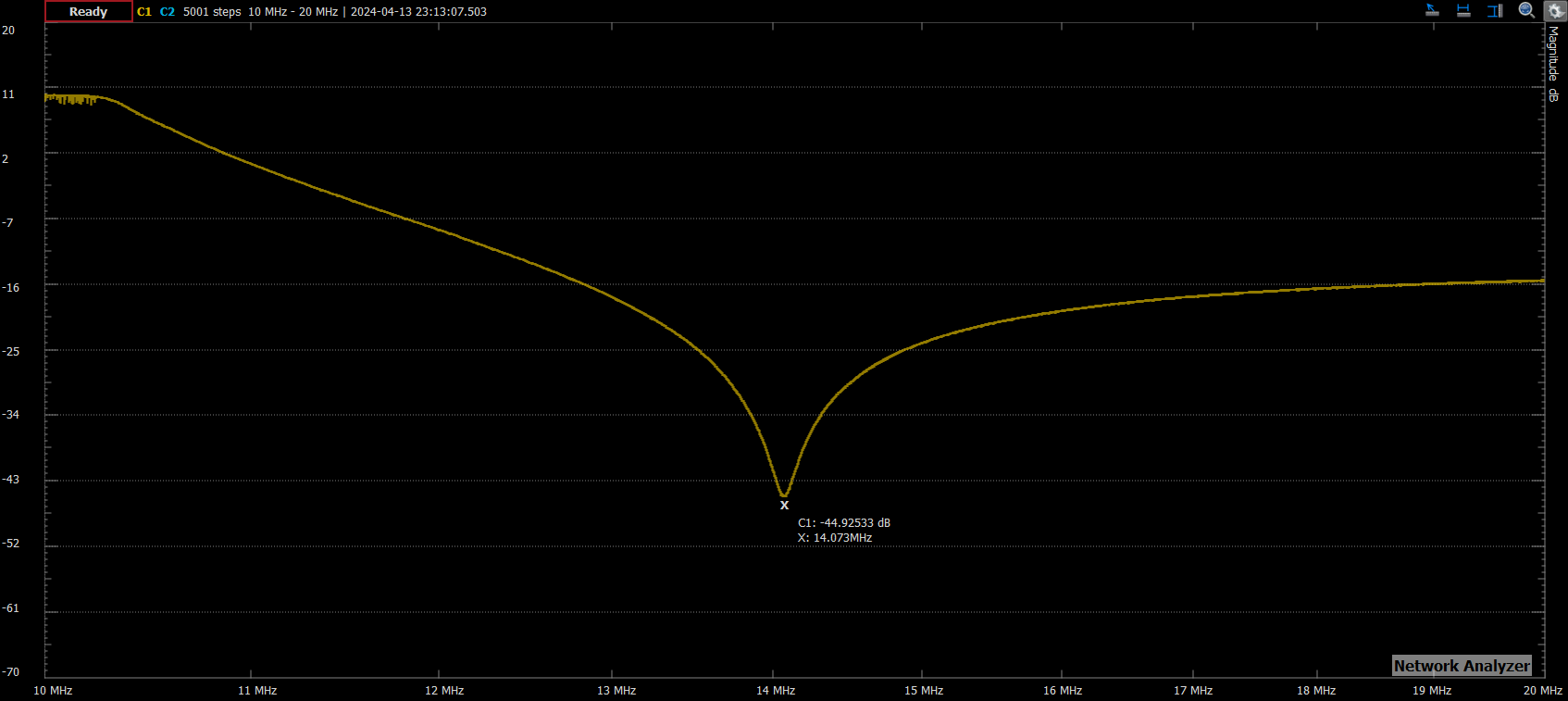
Network Analyzer
The above graph describes the S11 parameter, which represents the return loss of a device, indicating how much of the input power supplied to the device reflects back to the input port. We observe that at 14 MHz, the graph dips to a gain of -44.9 dB. This indicates that at 14 MHz, the magnitude of the reflected signal is lower than the magnitude of the incident signal. This implies that the antenna is absorbing the incident energy rather than reflecting it back towards the source. This response closely matches what we simulated previously in LTspice and MATLAB. For an NFC antenna, this behavior is desirable at 13.56 MHz. We can generate a graph with a dip closer to 13.56 MHz by including the tuning capacitor!
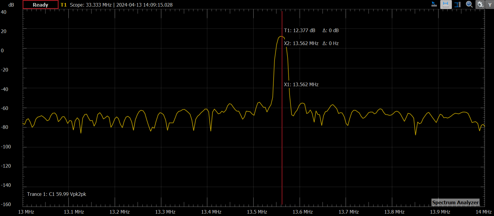
Spectrum Analyzer
Lastly, during the operation of the circuit, we can utilize the spectrum analyzer to observe the magnitude of the incoming signal. Keep in mind that this circuit doesn't contain a tuning capacitor. This was achieved by probing both ends of the antenna. Once a phone was brought within operating distance, we could see that the antenna contained a signal with a magnitude of 12.37 dB at 13.56 MHz.
By introducing a tuning capacitor with a value of 3.9pF, I was able to adjust the circuit's response to achieve resonance closer to the NFC standard of 13.56 MHz. Below is the graph produced by the network analyzer. We can see that this time the graph dips at a frequency of 13.555 MHz with a gain of -44.34 dB.
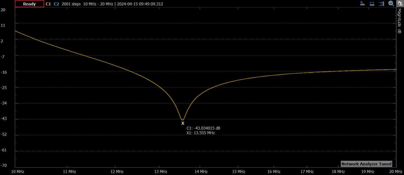
Network Analyzer
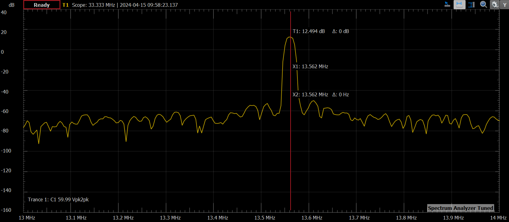
Spectrum Analyzer
Utilizing the same process as the previous spectrum analysis, we can observe that the antenna contained a signal with a magnitude of 12.494 dB at 13.562 MHz.
By introducing a really large tuning capacitor with a value of 15pF, we can adjust the circuit's response to achieve resonance at 12.5 MHz. Given the poorly tuned antenna, we expect to either see that the NFC capabilities cease to work or that the magnitude of the NFC signal is extremely weak. We can quantify this by utilizing the same spectrum analysis technique as used in the previous examples.
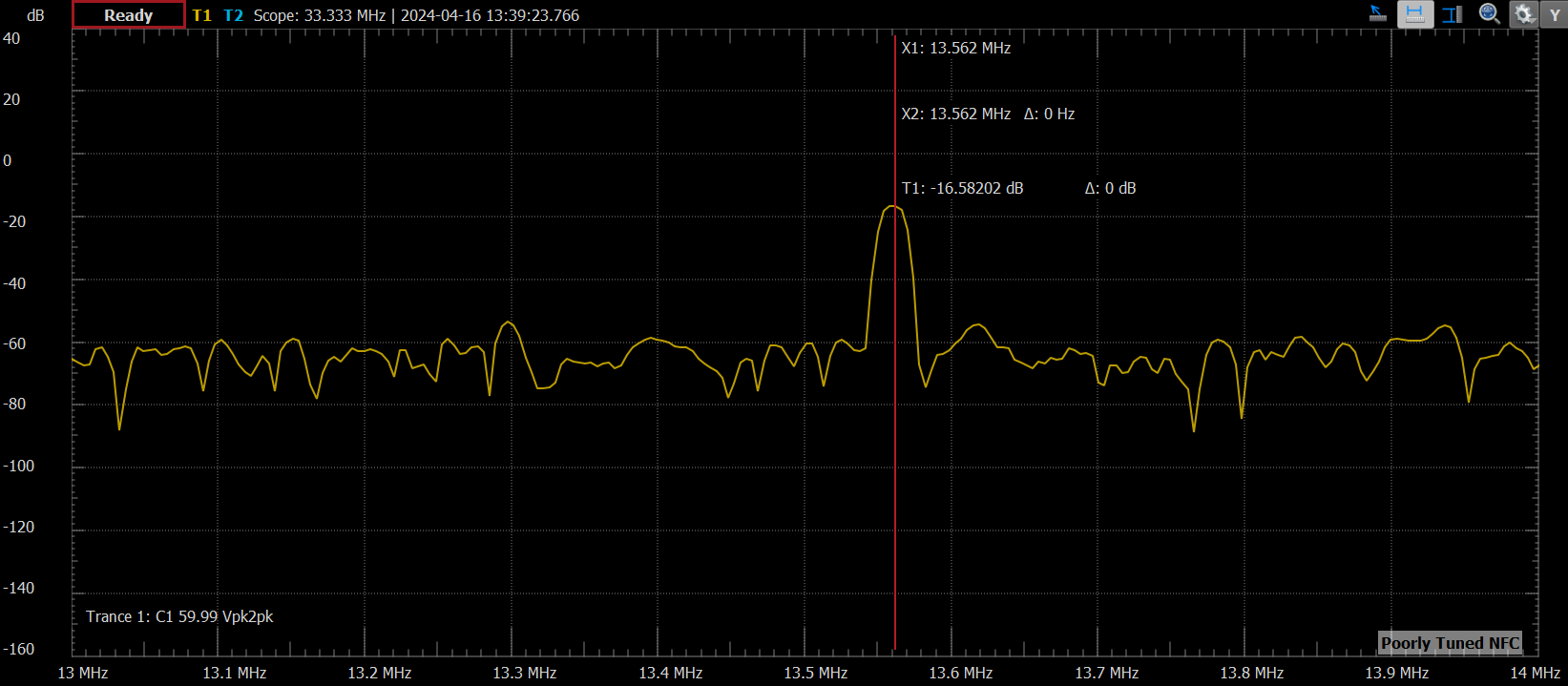
Spectrum Analyzer of Poorly Tuned Antenna
With the poorly tuned antenna, the NFC capabilities continued to work. However, it did require the phone to be slightly closer to the antenna. Additionally, based on the above graph, we can see that the magnitude of the NFC signal (13.56MHz) is significantly weaker than in previous examples.
By utilizing the Analog Discovery 2 oscilloscope feature, I was able to capture a snippet of an NFC transmission. This was done by probing the antenna during NFC operation. The NFC protocol is extremely complicated, and therefore, it is difficult to decipher what this transmission is. You can click on the following link to learn more about the NFC transmission protocol.
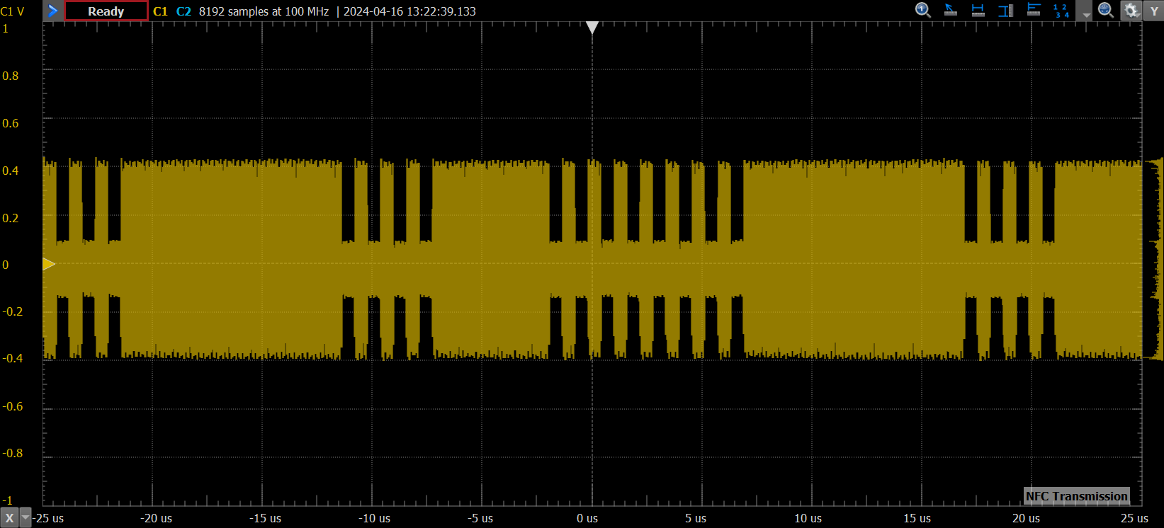
NFC Transmission
| Qty | Value | Footprint | References |
|---|---|---|---|
| 2 | LOGO | LOGO | G***, G*** |
| 1 | |||
| 1 | 220n | Capacitor_SMD:C_0603_1608Metric | C1 |
| 1 | 2p | Capacitor_SMD:C_0603_1608Metric | C2 |
| 1 | 47 | Resistor_SMD:R_0603_1608Metric | R1 |
| 1 | NT3H1101W0FTTJ | NT3H1101W0FTTJ:TSSOP8_SOT505-1_NXP | U1 |
| 1 | RED | LED_SMD:LED_0603_1608Metric | D1 |
The 8 most common of 9 parts.
AmirAlsad/beta-rush-pcb-cards
NFC + silkscreen PCB cards designed for MIT Beta Theta Pi rush week 2025 — KiCad sources, vendored library, and as-manufactured gerbers.

birbh/SmartTap
SmartTap is a sleek, credit card thin(.8mm) personal card powered entirely by NFC and its energy harvesting tech. i.e no battery required!!!


FrameworkComputer/ExpansionCards
Reference designs and documentation to create Expansion Cards for the Framework Laptop

VoronDesign/Voron-Hardware
Cool Hardware designed by the Voron Design group

hackclub/OnBoard
💡 Join 1,000 teenagers and make your first PCB with a $100 grant!

It measures 88.9 × 50.8 mm and has 2 copper layers, 1.6 mm thick.
9 parts, built around the NT3H1101W0FTTJ. The full list of its parts is on this page, with links to each part's symbol and footprint where PCBKit's library has them.
From the Raziz1/PCB_Business_Card repository on GitHub, at the commit this page was made from: the board is PCB_Business_Card.kicad_pcb and its schematic PCB_Business_Card.kicad_sch. PCBKit opens the board in the browser, with nothing to install.
Its repository states no licence, so its author keeps all rights: ask Raziz1 before reusing the design.