
2 layers88.9 × 50.8 mm
PCB Business Card
AmirAlsad/beta-rush-pcb-cards
NFC + silkscreen PCB cards designed for MIT Beta Theta Pi rush week 2025 — KiCad sources, vendored library, and as-manufactured gerbers.
10 parts

 AmirAlsad/beta-rush-pcb-cards
NFC + silkscreen PCB cards designed for MIT Beta Theta Pi rush week 2025 — KiCad sources, vendored library, and as-manufactured gerbers.
PCB Business Card is an open-source printed circuit board by AmirAlsad, from the AmirAlsad/beta-rush-pcb-cards repository on GitHub. It is a 2-layer board of 88.9 × 50.8 mm with 11 parts on 7 nets, routed with 12 tracks and 0 vias.
It is built around the NT3H1101W0FTTJ. Its parts include 2 capacitors, 1 resistor, 1 IC and 1 diode. It belongs with the radio and wireless boards of this library.
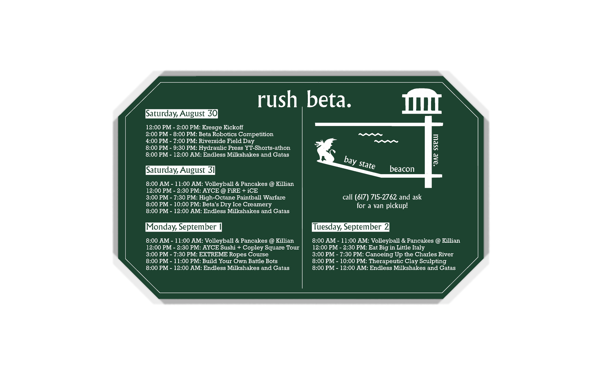
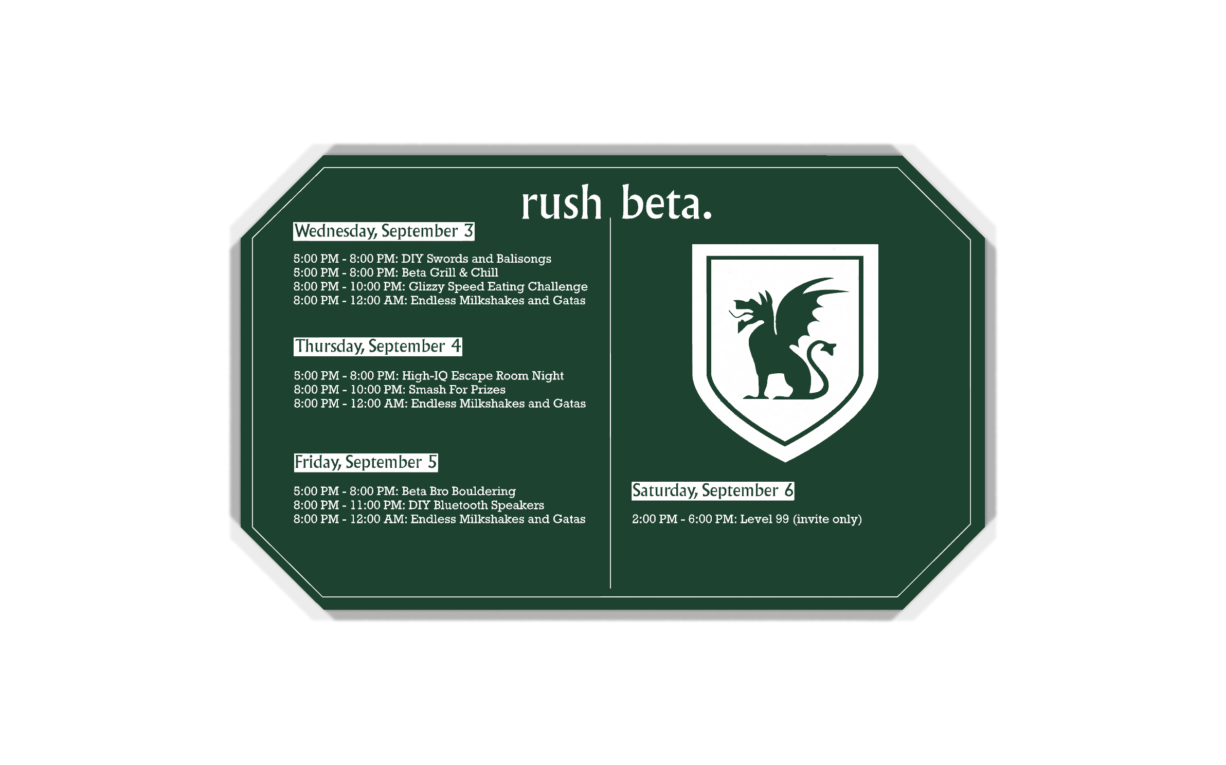
Handed to PNMs (prospective new members) during rush. It's a PCB purely as a gimmick — there is no circuit here at all: no components, no nets, no copper routing. The schematic is an empty sheet. Everything you see is silkscreen on a bare two-layer board.
That makes this the easy card to reuse: nothing electrical can break, and the only work each year is retyping the schedule.
| Source of record | PNM_Rush_Card.kicad_pcb, last saved 2025-07-30 |
| Designed in | KiCad 9.0.2 |
| Outline | 89.98 × 54.97 mm, octagonal (clipped corners) |
| Stackup in the file | 2 layer FR4, 1.6 mm |
| As actually ordered | 1 mm thick, green mask, white silkscreen — 350 pcs, $86.10 |
| Layers used | F.SilkS (28 items), B.SilkS (22), Edge.Cuts (8), one placeholder item each on F.Cu / B.Cu |
| Fab package | fab/2025-07-30_release/ — byte-identical to what JLCPCB received |
| Order record | ../docs/order-history.md |
The file says 1.6 mm; the cards are 1 mm. Thickness is an order-page setting that isn't carried in the gerbers, so nothing reconciles it automatically. Set 1 mm explicitly on a reorder or you'll get noticeably chunkier cards.
The corners are chamfered — Edge.Cuts is an octagon, not a rectangle. A
rectangular card can be sheared or V-scored cheaply; this profile has to be
routed. When quoting, make sure the vendor is pricing a routed outline and
isn't silently substituting a rectangle. This is the single most likely way a
reorder comes back looking wrong.
JLCPCB got this right in 2025: its production file set for this card contains no V-cut layer at all (and no drill file, since there are no holes), confirming the profile was routed as intended. The brother card's set, by contrast, does have a V-cut layer — for the assembly edge rails.
Front — rush beta., the Back Bay map (MIT dome, Mass Ave, Charles, Bay
State, Beacon), call (617) 715-2762 and ask for a van pickup!, and the first
four days:
| Day | Events |
|---|---|
| Saturday, August 30 | Kresge Kickoff · Beta Robotics Competition · Riverside Field Day · Hydraulic Press YT-Shorts-athon · Endless Milkshakes and Gatas |
| "Saturday, August 31" ⚠️ | Volleyball & Pancakes @ Killian · AYCE @ FiRE + iCE · High-Octane Paintball Warfare · Beta's Dry Ice Creamery · Endless Milkshakes and Gatas |
| Monday, September 1 | Volleyball & Pancakes @ Killian · AYCE Sushi + Copley Square Tour · EXTREME Ropes Course · Build Your Own Battle Bots · Endless Milkshakes and Gatas |
| Tuesday, September 2 | Volleyball & Pancakes @ Killian · Eat Big in Little Italy · Canoeing Up the Charles River · Therapeutic Clay Sculpting · Endless Milkshakes and Gatas |
Back — rush beta., the crest, and the rest of the week:
| Day | Events |
|---|---|
| Wednesday, September 3 | DIY Swords and Balisongs · Beta Grill & Chill · Glizzy Speed Eating Challenge · Endless Milkshakes and Gatas |
| Thursday, September 4 | High-IQ Escape Room Night · Smash For Prizes · Endless Milkshakes and Gatas |
| Friday, September 5 | Beta Bro Bouldering · DIY Bluetooth Speakers · Endless Milkshakes and Gatas |
| Saturday, September 6 | Level 99 (invite only) |
⚠️ A typo shipped on the physical cards. The second block reads "Saturday, August 31", but August 31, 2025 was a Sunday. Every other day label is correct. It is left uncorrected in the source so this archive matches the object that was actually handed out — fix it when you retype the dates for a new year.
Same technique as the brother card: art is polygons inside footprints, generated
with KiCad's Bitmap to Component converter. This board places btp:map (from the
vendored ../lib/) and one wordmark/crest footprint whose library link
is the stale bare name LOGO — it lives inside the .kicad_pcb and plots
correctly, but can't be updated from library. Don't delete it casually.
Event text is ordinary KiCad text objects with embedded \n line breaks, which is
what makes this card straightforward to retype — see
../docs/next-year-checklist.md.
KiCad 10 reports 21 violations, all text_thickness, and nothing else: no
clearance errors, no unconnected items, no parity errors. The warnings say the
silkscreen stroke width is below the 0.15 mm design rule. The fab printed them
legibly anyway, as the renders show.
If you shrink the text further to fit more events, that warning is the thing to actually pay attention to — at some point thin silkscreen stops resolving and becomes unreadable. Keep an eye on the smallest strokes and ask the vendor for their real minimum line width.
fab/2025-07-30_release/ holds the gerbers that were
sent out: F.Cu, B.Cu, both silkscreens, both masks, both pastes, Edge.Cuts,
and two drill files (both empty — there is nothing to drill). Plotted from
KiCad 9.0.2; the job file reports 90.03 × 55.02 mm.
These have been byte-compared against the files JLCPCB actually received and are identical, so reordering from this folder reproduces the 2025 cards exactly.
One aesthetic note: the order specified Mark on PCB: Order Number, and unlike the brother card this one has no edge rails for JLCPCB to hide that marking on. There is probably a small JLCPCB order number printed somewhere on a face of the delivered cards. If that matters, pick "Remove order number" or specify a location next time.
The silkscreen gerbers are large (1.1 MB front, 658 KB back) because all that text and artwork is flattened to polygons. That's normal, not corruption.
| Qty | Value | Footprint | References |
|---|---|---|---|
| 1 | |||
| 1 | 220n | Capacitor_SMD:C_0603_1608Metric | C1 |
| 1 | 2p | Capacitor_SMD:C_0603_1608Metric | C2 |
| 1 | 65 | Resistor_SMD:R_0603_1608Metric | R1 |
| 1 | LOGO | btp:map | G*** |
| 1 | LOGO | btp:doodles | G*** |
| 1 | LOGO | btp:btp-text-footprint-lg | G*** |
| 1 | LOGO | btp:btp-dragon-footprint | G*** |
| 1 | NT3H1101W0FTTJ | Package_SO:TSSOP-8_3x3mm_P0.65mm | U1 |
| 1 | RED | LED_SMD:LED_0603_1608Metric | D1 |
The 10 most common of 11 parts.
AmirAlsad/beta-rush-pcb-cards
NFC + silkscreen PCB cards designed for MIT Beta Theta Pi rush week 2025 — KiCad sources, vendored library, and as-manufactured gerbers.

Raziz1/PCB_Business_Card
A PCB business card with NFC capabilities designed in KiCad

birbh/SmartTap
SmartTap is a sleek, credit card thin(.8mm) personal card powered entirely by NFC and its energy harvesting tech. i.e no battery required!!!

google/mozc-devices
Circuit diagrams and firmware source code for Gboard DIY keyboards


FrameworkComputer/ExpansionCards
Reference designs and documentation to create Expansion Cards for the Framework Laptop

hoglet67/RGBtoHDMI
Bare-metal Raspberry Pi project that provides pixel-perfect sampling of Retro Computer RGB/YUV video and conversion to HDMI

hackclub/OnBoard
💡 Join 1,000 teenagers and make your first PCB with a $100 grant!

It measures 88.9 × 50.8 mm and has 2 copper layers, 1.6 mm thick.
11 parts, built around the NT3H1101W0FTTJ. The full list of its parts is on this page, with links to each part's symbol and footprint where PCBKit's library has them.
From the AmirAlsad/beta-rush-pcb-cards repository on GitHub, at the commit this page was made from: the board is brother-card-v1/PCB_Business_Card.kicad_pcb and its schematic brother-card-v1/PCB_Business_Card.kicad_sch. PCBKit opens the board in the browser, with nothing to install.
Its repository states no licence, so its author keeps all rights: ask AmirAlsad before reusing the design.