
2 layers132.1 × 45.7 mm
IPoS
peterheinrich/InternetOverSpaghetti
Transmitting IP packages over a pair of spaghetti thus demonstrating how media independent IP really is.
42 parts342

 Quee0/Ignis-overdrive1
Ignis overdrive guitar effect
Overdrive effect is an open-source printed circuit board by Quee0, from the Quee0/Ignis-overdrive repository on GitHub. It is a 2-layer board of 65 × 99 mm with 47 parts on 24 nets, routed with 120 tracks and 0 vias.
It is built around the LM358. Its parts include 9 capacitors, 6 resistors, 5 diodes, 4 switches and 1 IC. It belongs with the audio and music boards of this library.




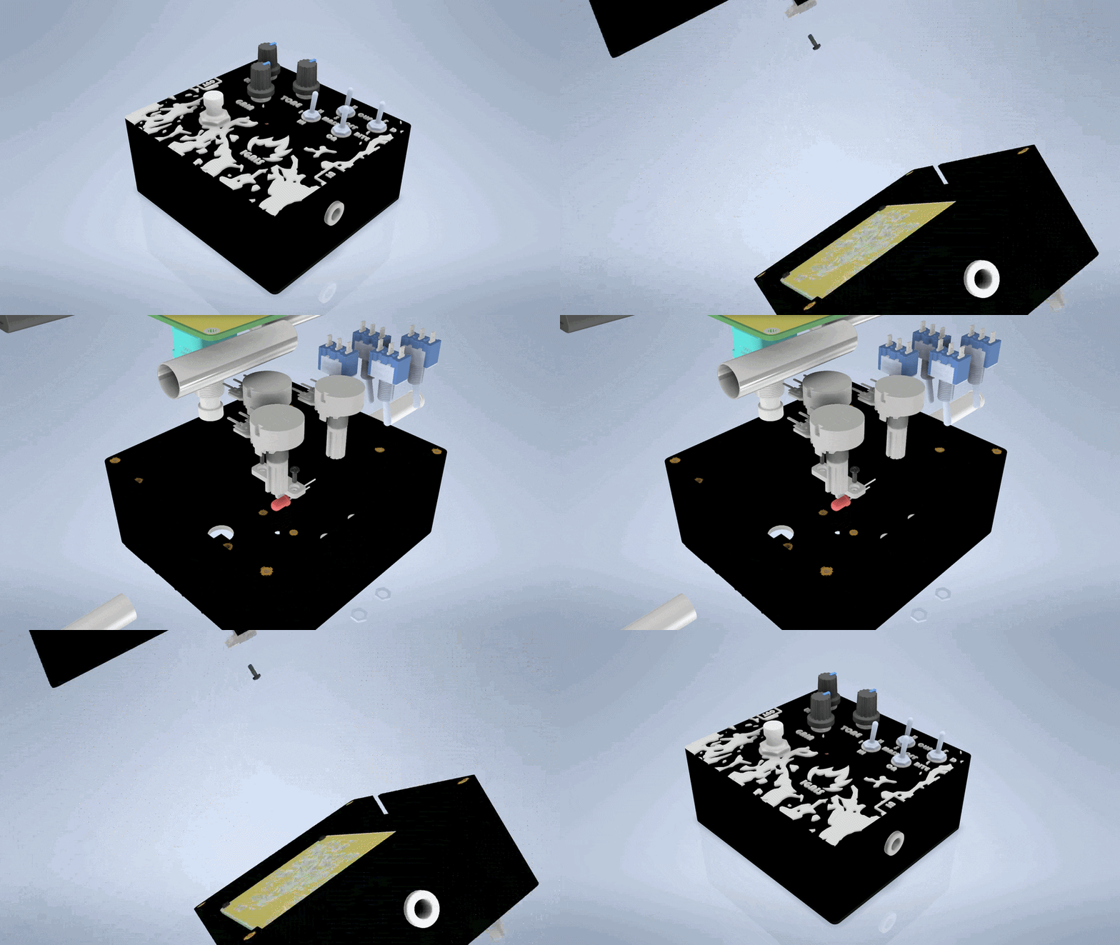
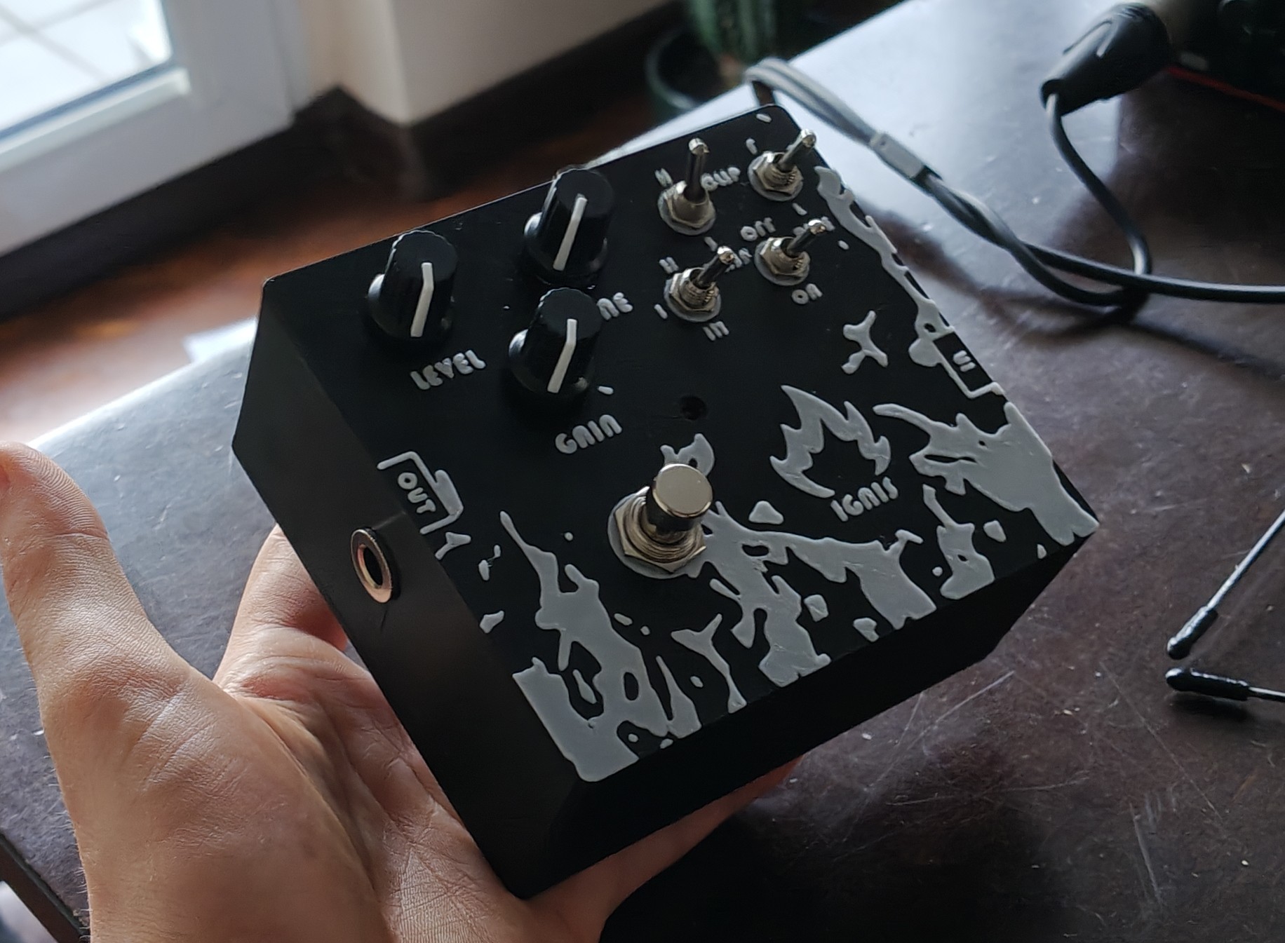
This project presents the complete design and mathematical analysis of a versatile, fully analog overdrive guitar pedal built around an operational amplifier. At its core, the main amplification block delivers a massive voltage gain (up to 1000x), paired with a flexible multi segmented tonal shaping section.
[!NOTE] This includes:
- Hardware pre-amp bass switch to modify the low-end structure before clipping,
- Low-pass pre-amp filter integrated into the feedback loop, it actively works with gain and can be switched on and off,
- Customizable clipping: fast-switching silicon diodes and LEDs, hard and soft clipping.
- Final refinements through a classic passive Tone control (lowpass filter),
- Master volume stage with DC-blocking (static high pass filter),
The end result is a highly customizable overdrive capable of spanning from a transparent, mid-focused crunch to a thick, saturated lead tone, demonstrating a practical understanding of circuit design and mathematical theory usage.
https://github.com/user-attachments/assets/1be89b33-93ce-4a43-86b3-0c42de0525c9
https://github.com/user-attachments/assets/2ba2562c-e011-4fdd-8f06-044c0ea2faf1
https://github.com/user-attachments/assets/6c816d3a-e20a-423a-b53f-dbef71fd2bd0
https://github.com/user-attachments/assets/7a0f3d32-2f00-4b13-9497-afda9a19c826
https://github.com/user-attachments/assets/31108739-4f4a-404e-89c9-3ae1a5144b9c
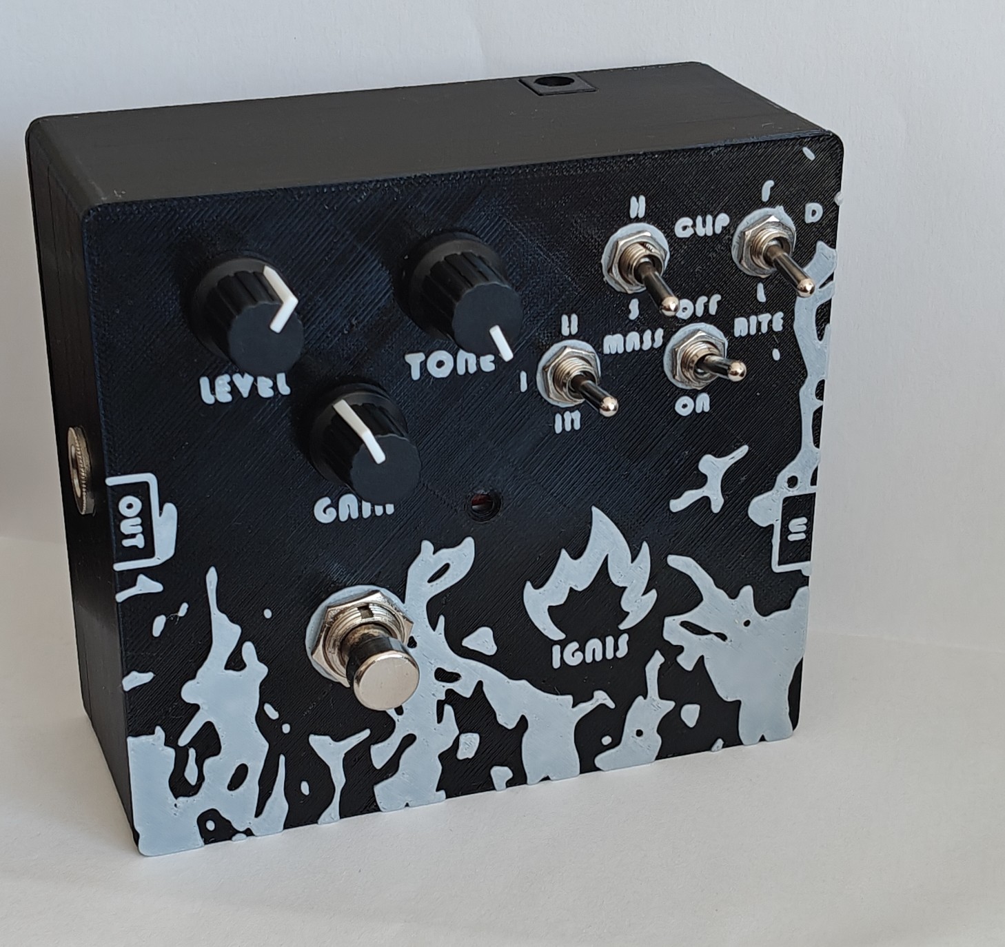
Enable / disable guitar effect,Hard / Soft Clipping mode toggle. Note: Different clipping modes inherently yield different overall volume and compression levels. You will likely need to compensate with the Level knob.Fast-switching / None / LED choose cliping diodes,II / I / III choose how massive you want the tone to be, how much to amplify the bass.Off / On Engages the feedback-loop smoothing capacitor (100pF). Turn it ON to roll off harsh high-end fizz and soften the overall clipping behavior.
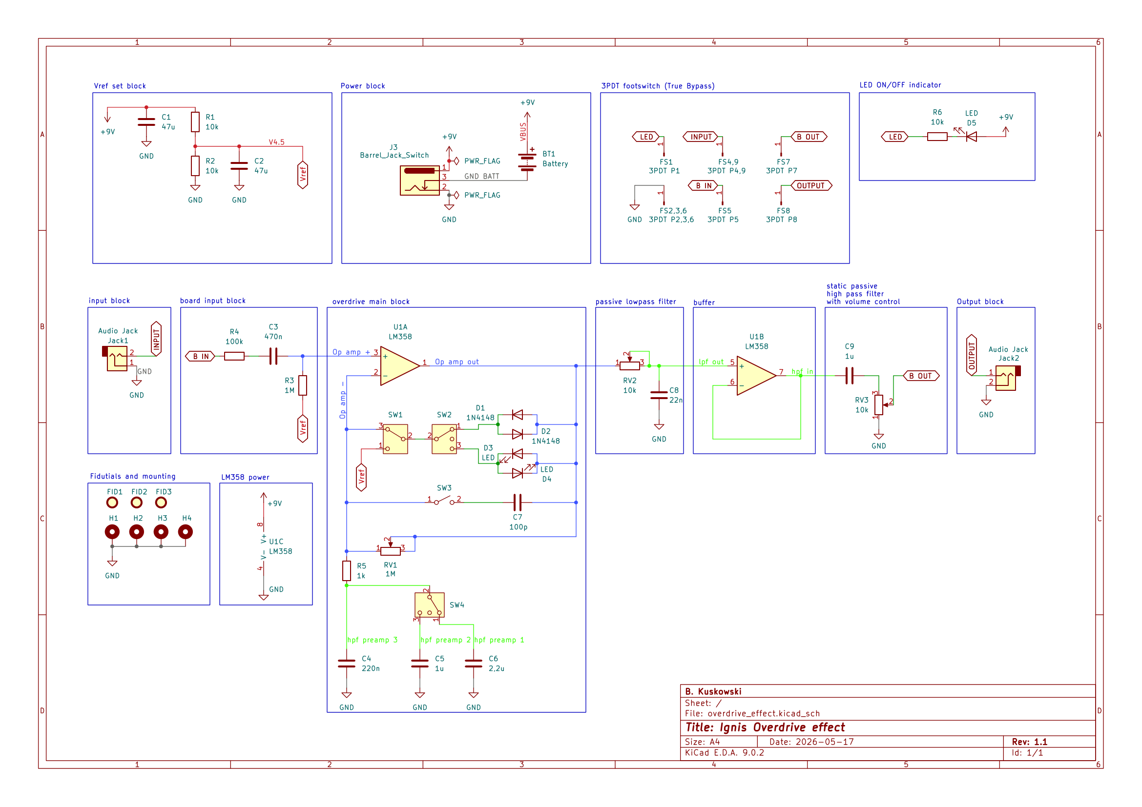
Block Diagram Explanation
[!NOTE] Upon later revision there are 2 possible further impovements:
- While setting $V_{ref}$ use buffor to further stabilize reference potential point.
- Add protective resistance to output of an op amp in main overdrive block.
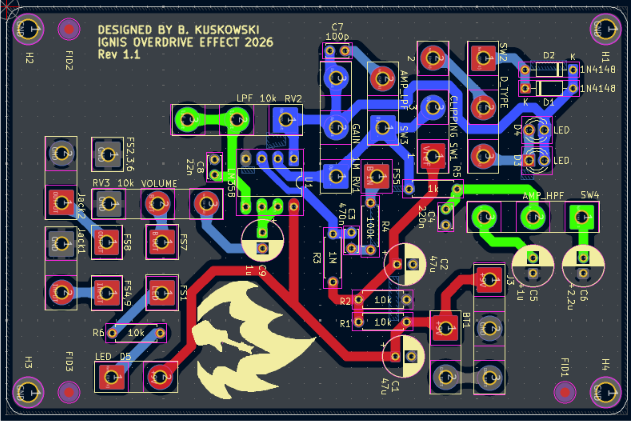
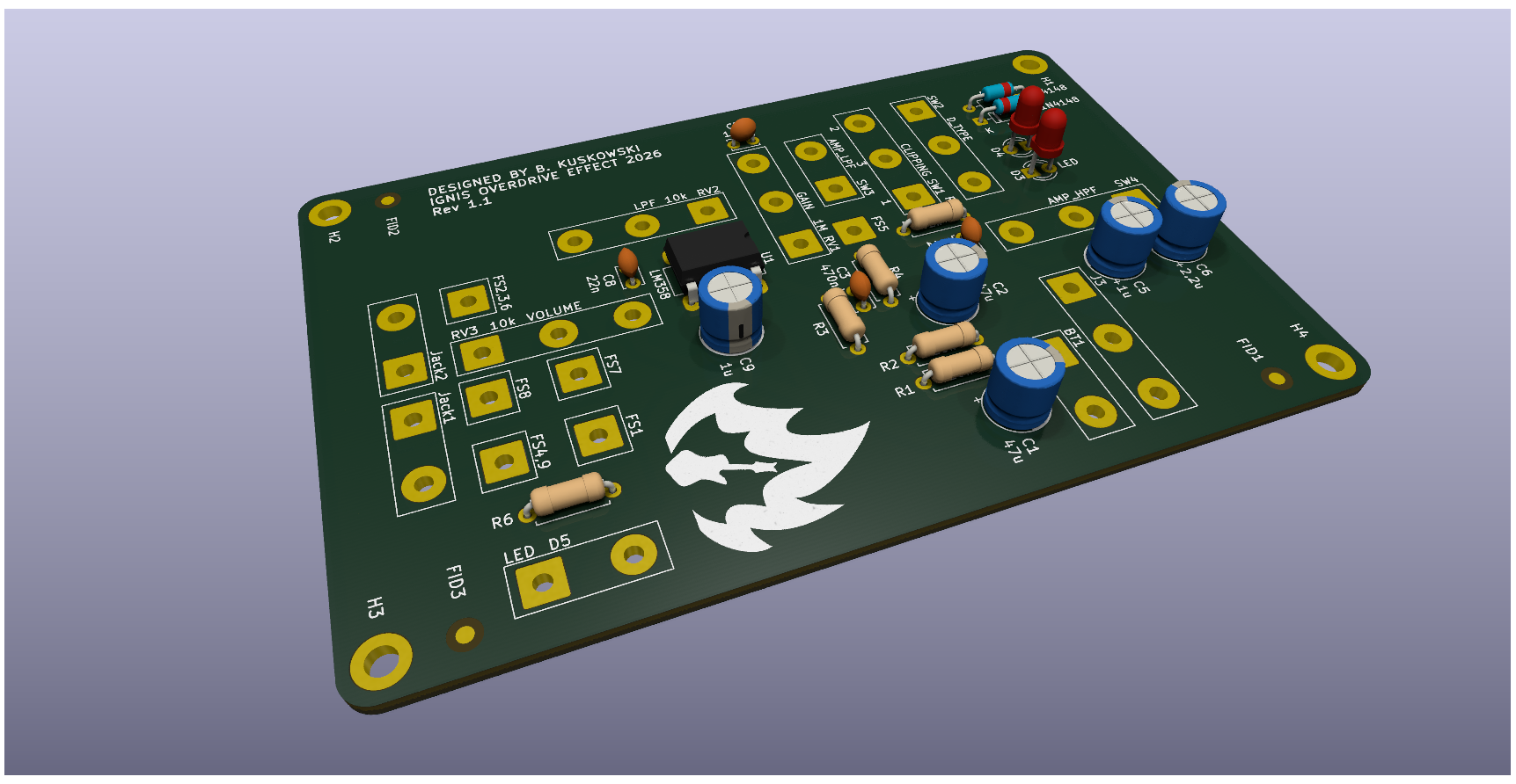
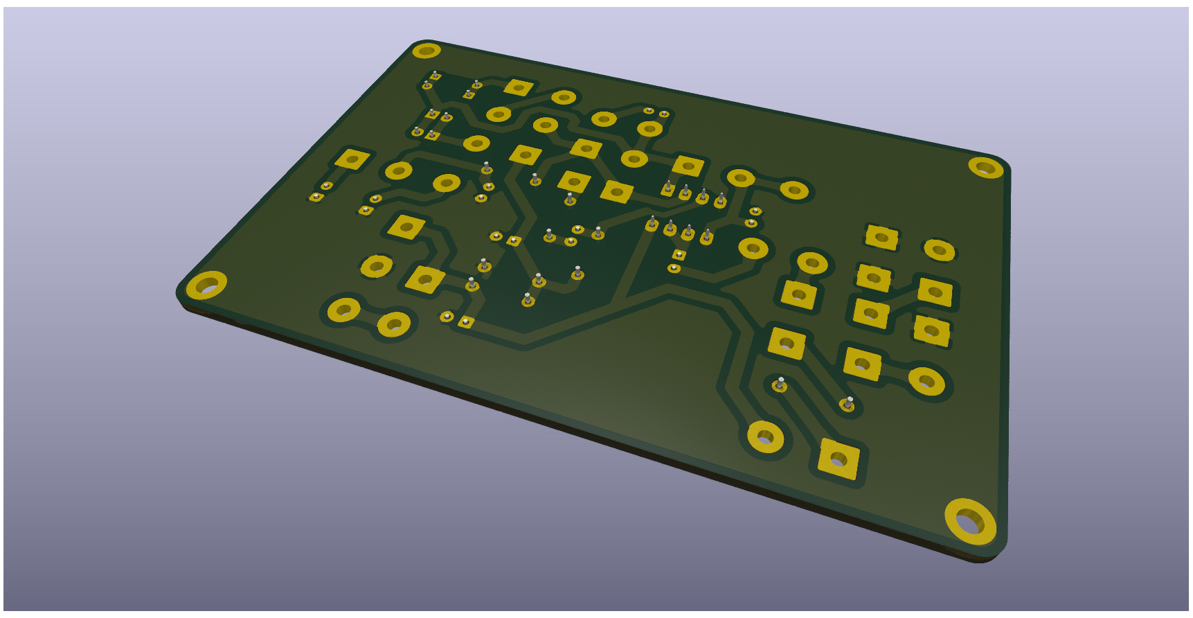
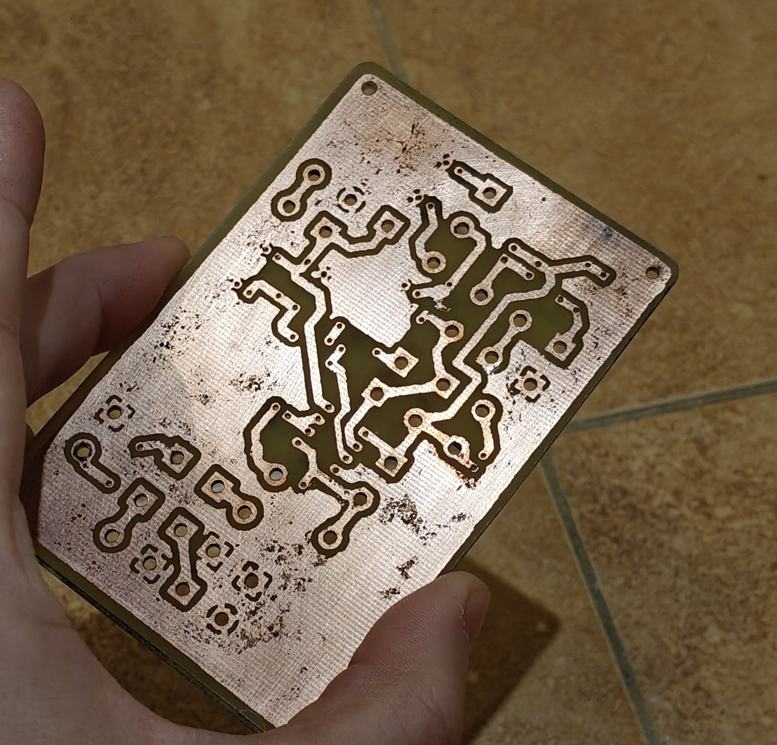
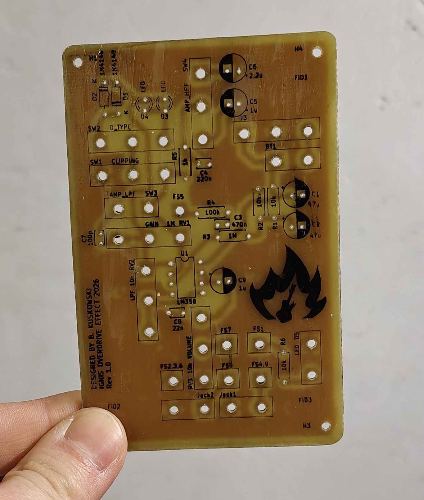
PCB Layout Features. Designed for maximum audio integrity, mechanical reliability, and DIY accessibility:
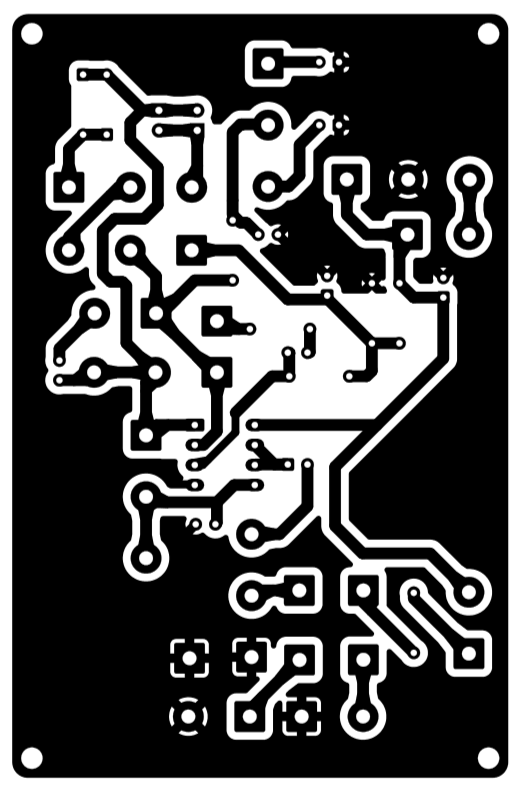
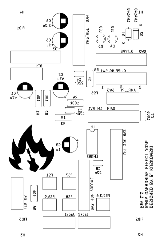
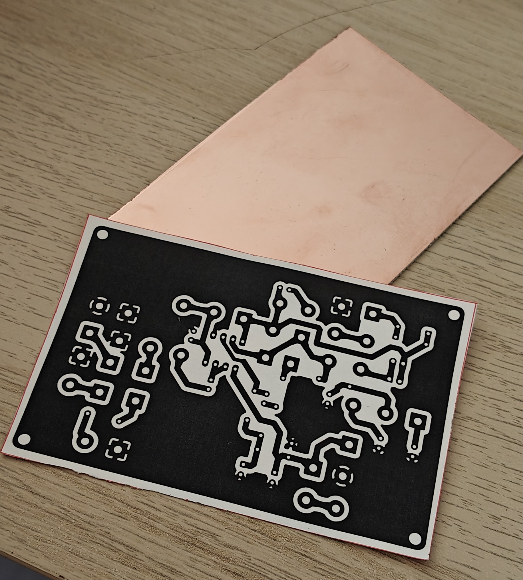
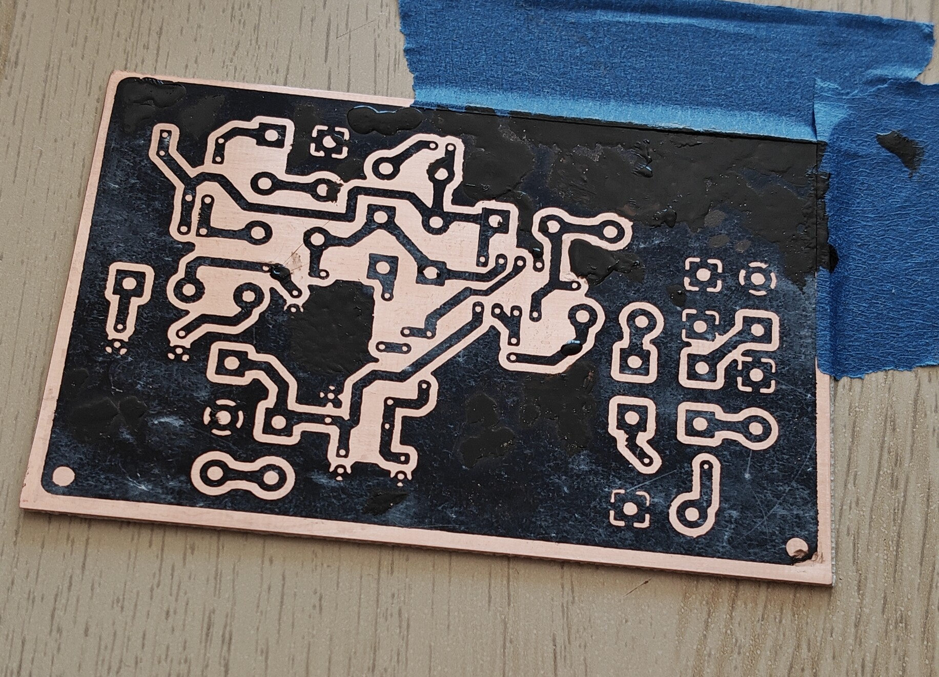
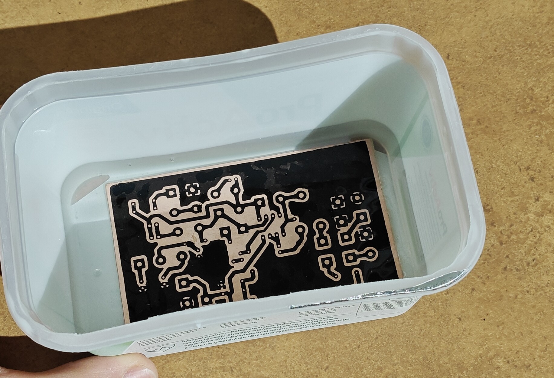
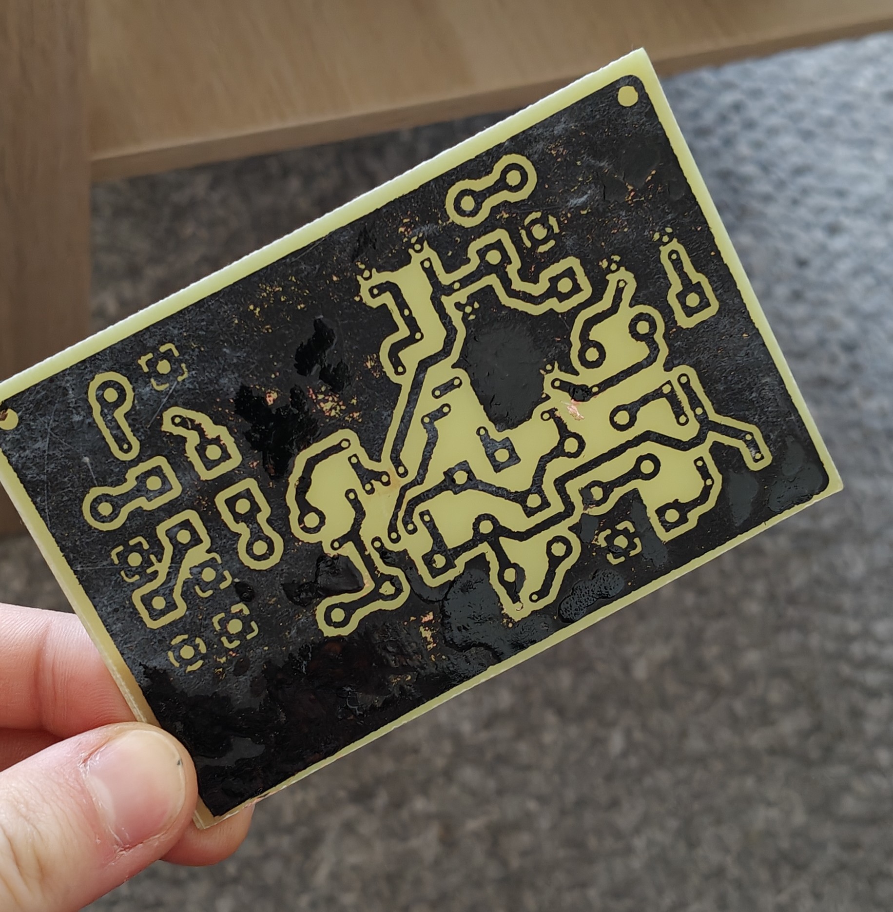
PNGs of files ready to thermotransfer (pdfs in img\import)
In this derivation we consider loaded decoupling capacitor which makes lowpass filter (integrating circuit). The last derived equation in 3.1 is identical for coupling capacitor working with resistance (differentiating circuit), but it is different on laplace's s-domain, and in fourier analysis (phase and magnitude plots).
$$U_{out}=U_{in} \cdot \frac{Z_L}{Z_L+Z_R}$$
$$U_{out}=U_{in} \cdot \frac{\frac{Z_C Z_{Ro}}{Z_C+Z_{Ro}}}{\frac{Z_C Z_{Ro}}{Z_C+Z_{Ro}}+Z_R} = U_{in} \cdot \frac{Z_C Z_{Ro}}{Z_C Z_{Ro}+Z_C Z_{R}+Z_RZ_{Ro}}$$
Definition of Laplace's transform:
$$F(s) = L[f(t)] = \int_{0}^{\infty} f(t) e^{-st} , dt \Rightarrow L\left[\frac{d^nf(t)}{dt^n}\right] = s^nF(s)$$
considering no initial conditions.
Impedance of resistance $Z_R$:
$$U=I\cdot R$$
$$L[U]=R\cdot L[I]$$
$$Z_R(s)=\frac{U(s)}{I(s)}=R$$
Impedance of capacitance $Z_C$:
$$I=C\cdot \frac{dU}{dt}$$
$$L[I]=C\cdot L[U']$$
$$I(s)=C\cdot sU(s)$$
$$Z_C(s)=\frac{U(s)}{I(s)}=\frac{1}{sC}$$
$$G(s)=\frac{U_{out}}{U_{in}}=\frac{\frac{R_o}{sC}} {\frac{R_o}{sC}+\frac{R}{sC}+RR_o}=\frac{R_o}{R_o+R+sCRR_o}$$
$$G(s)=\frac{(\frac{R_o}{R_o+R})}{1+s(\frac{CRR_o}{R_o+R})}$$
Then:
$$\boxed{G(s)=\frac{K}{1+sT}},\qquad \boxed{K=\frac{R_o}{R_o+R}},\qquad \boxed{T=\frac{CRR_o}{R_o+R}}$$
Complex s-plane argument definition: $s = \sigma+j\omega$. To get amplitude characteristic we need to analyse holomorphic Fourier transform function. To achieve that we need to get rid of real part of s-plane (constant component $e^\sigma$).
$$G(j\omega)=\frac{K}{1+j\omega T}\cdot\frac{1-j\omega T}{1-j\omega T}=\frac{K-j\omega KT}{1+\omega^2 T^2}$$
$$G(j\omega)=\left[\frac{K}{1+\omega^2 T^2}\right] + j\left[\frac{-\omega KT}{1+\omega^2 T^2}\right]$$
$P(\omega)\left[Q(\omega)\right]$ characteristics:
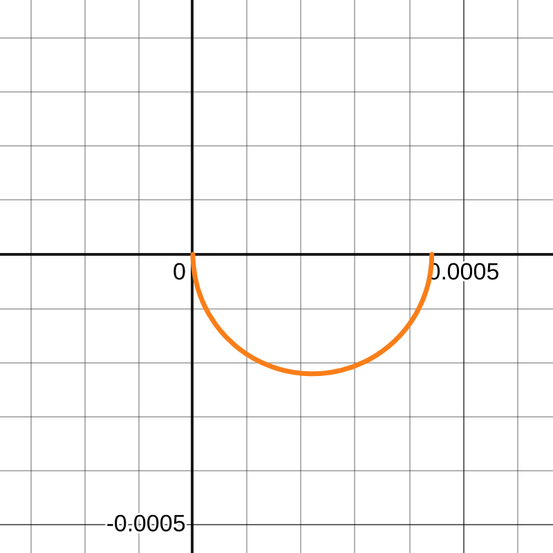
(https://www.desmos.com/calculator/vwyactze44)
To derive amplitude-frequency function we must analyse mod.$$|G(j\omega)|=\sqrt{\frac{K^2}{(1+\omega^2 T^2)^2}+\frac{\omega^2 K^2 T^2}{(1+\omega^2 T^2)^2}}=\frac{K}{\sqrt{1+\omega^2 T^2}}$$
Finding -3dB frequency will be done based on magnitude.
$$A=20\cdot \log\left(\frac{K}{\sqrt{1+\omega^2 T^2}}\right)$$
Cutoff condition:
$$A(\omega_{-3dB})=A(0)-3$$
$$20\cdot \log\left(\frac{K}{\sqrt{1+\omega^2 T^2}}\right)=20\cdot \log\left(\frac{K}{\sqrt{1+0^2 T^2}}\right)-3$$
$$10\left[\log\left(\frac{K^2}{(1+\omega^2 T^2)}\right)-\log\left(K^2\right)\right]=-3$$
$$\log\left(\frac{1}{(1+\omega^2 T^2)}\right)=-0,3$$
$$\frac{1}{(1+4\pi^2f^2 T^2)}=10^{-0,3}$$
$$10^{-0,3}+10^{-0,3}4\pi^2f^2 T^2=1$$
$$f=\sqrt{\frac{\frac{10^{-0,3}}{1-10^{-0,3}}}{4\pi^2T^2}} \approx \frac{1}{2\pi T}$$
Substitute T:
$$f=\frac{R_o+R}{2\pi CRR_o}=\frac{R}{2\pi CRR_o}+\frac{R_o}{2\pi CRR_o}$$
$$\boxed{f=\frac{1}{2\pi RC}+\frac{1}{2\pi R_oC}}$$
We consider loaded symetric voltage divider
$$R_{eq1}=\frac{RR_o}{R+R_o}$$
$$\lim_{R_o \to \infty} R_{eq1}= \lim_{R_o \to \infty}\frac{R}{\frac{R}{R_o}+1}=R$$
$$R_{eq}=2\cdot R$$
$$I=\frac{V_{cc}}{R_{eq}}=\frac{V_{cc}}{2R}$$
$$R_{TH}=\frac{RR}{R+R}=\frac{R}{2} \Rightarrow R = 2\cdot R_{TH}$$
Substituting both equations:
$$\boxed {I(R_{TH})=\frac{V_{cc}}{4\cdot R_{TH}}}$$
Ideal voltage source should have $R_{TH} \to 0$, to be as stable as possible. Ideal current loss should be $I \to 0$. Graphing this function allow to pick optimal resistance values.
$I(R_{TH})$ with $V_{cc}=9V$ characteristics:
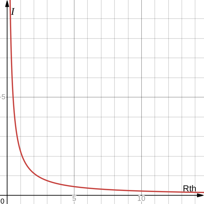
(https://www.desmos.com/calculator/zl9quwhx7r)
Considering methodology of choosing pullup resistors, low potential on signal line should not draw much current. On the other hand, operational amplifier has its bias current which will be drawn no matter what. It limits upper value of resistance, voltage drop on this resistor should not affect effect.
In project LM358 was used, so its bias current is around $45 nA = 45\cdot 10^{-9} A$
$$U = I\cdot R$$
$$R = \frac{U_{loss}}{45\cdot 10^{-9}}$$
Characteristics:
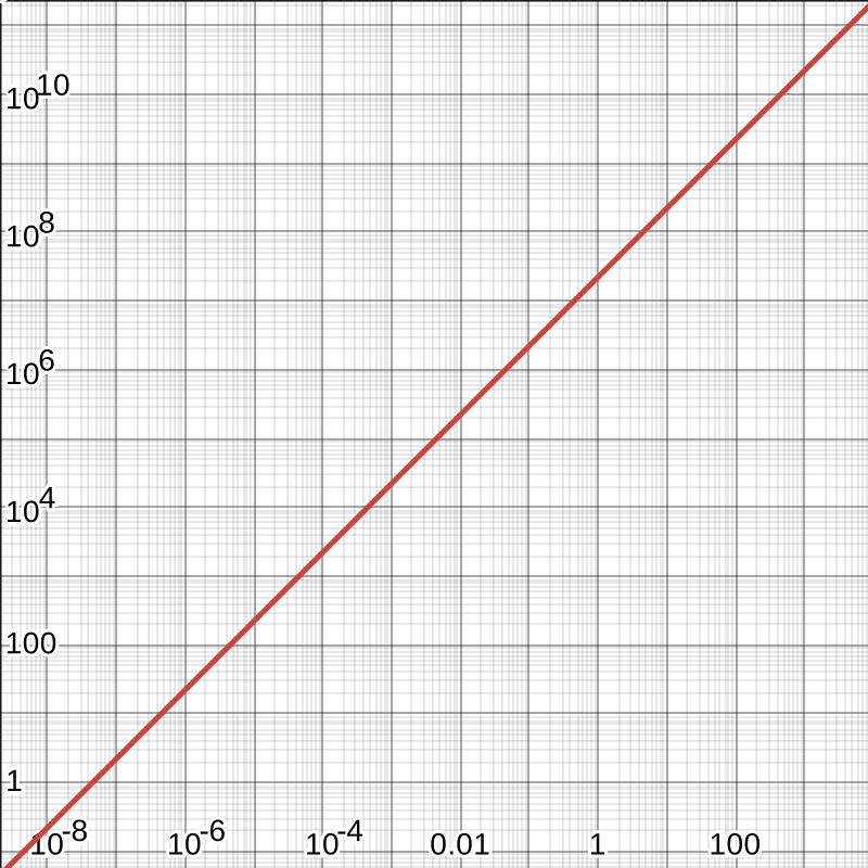
(https://www.desmos.com/calculator/fuyu1ywsum)
Op amps has very high input impedance ($Z_{in} \to \infty$) and very low output impedance ($Z_{out} \to 0$). They can be analysed using 2 rules:
Using 2 rules, non-inverting amp can be modeled with:
$$U_{in} = U_{+} = U_{-} = Z_1 \cdot I$$
$$U_{out} = U_{Z_1} + U_{Z_2} = I\cdot Z_1 + I\cdot Z_2 \Rightarrow I = \frac{U_{out}}{Z_1 + Z_2}$$
$$G(s) = \frac{Z_2 (s)}{Z_1(s)} + 1$$
In this effect we are enabling user to regulate $Z_2$ (diode type, potentiometer and capacitor). We use capacitor $C_4$ to limit gain for DC current. Considering only $1M\Omega$ potentiometer and using information derived in 3.1:
$$G(s) = \frac{R_{V1}}{R_5+ \frac{1}{sC_4}} + 1 = \frac{sR_{V1} C_4}{sR_5 C_4 + 1} + 1 = \frac{1 + sC_4(R_{V1} + R_5)}{1 + sR_5C_4}$$
To calculate gain in somewhat same way that we derived 3.1 $s = j\omega$ :
$$G(j\omega) = \frac{1 + j\omega C_4(R_{V1} + R_5)}{1 + j\omega R_5C_4} = [\frac{1+\omega^2 C_4^2 R_5 (R_{V1}+R_5)}{1+\omega^2 R_5^2 C_4^2}] + j [\frac{\omega C_4 R_{V1}}{1+\omega^2 R_5^2 C_4^2}]$$
$$|G(j\omega)| = \sqrt{Re[G(j\omega)]^2+Im[G(j\omega)]^2} = \sqrt{\frac{1 + \omega^2 C_4^2(R_{V1} + R_5)^2}{1 + \omega^2 R_5^2 C_4^2}}$$
So impedance for DC current is:
$$\lim_{\omega \to 0} |G(j\omega)| = 1$$
So impedance for high frequency AC current is:
$$\lim_{\omega \to \infty} |G(j\omega)| = \frac{R_{V1}}{R_5} + 1$$
Using $I(R_{TH})=\frac{V_{cc}}{4\cdot R_{TH}}\qquad$ (3.2). Voltage divider should not drain more than $0.5 mA$, so:
$$0.5 \cdot 10^{-3} > \frac{9}{4\cdot R_{TH}}$$
$$2 \cdot 10^{-3} \cdot R_{TH} > 9$$
$$R_{TH} > 4,5 \cdot 10^3 \Rightarrow R_{1,2} > 9 k\Omega$$
$$\boxed{R_{1,2} = 10 k\Omega}$$
Using $R = \frac{U_{loss}}{45\cdot 10^{-9}}$ (3.4). Maximal acceptable voltage drop is around $0.05 V$, so:
$$R_3 = \frac{0,05}{45\cdot 10^{-9}} \approx 1,111 \cdot 10^6 \Omega \approx 1 M\Omega$$
$$\boxed{R_3 = 1M\Omega}$$
It is standard current and voltage limiting resistor.
$$\boxed{R_4 = 100k\Omega}$$
Potentiometers were chosen based on availability and functionality. Picking $10k\Omega$ potentiometers grants optimal selection of coupling and decoupling capacitors to work with (look 4.5). Also in main feedback loop there is main bass level control, so not to do too many knobs we stuck to a static highpass filter. It also works with $10k\Omega$ potentiometer as volume control. it gives relatively low internal resistance of an effect.
$$\boxed{R_{V2,V3} = 10k\Omega}$$
Gain potentiometer was also chosen based on construction standards, but to make effect more customizable we chose $1M\Omega$ which grants more boost.
$$\boxed{R_{V1} = 1M\Omega}$$
Decoupling $9V$ source and $4.5V$($V_{ref}$) after voltage divider is done by $C_1$ and $C_2$. Values were chosen using Thevenin's method.
Capacitor $C_2$ works with $5 k\Omega$ resistance, we want to cutoff frequencies all above $0.01 Hz$:
$$R_{TH} = \frac{10k \cdot 10k}{10k + 10k} = 5k\Omega$$
$$C_2 > \frac{1}{2\pi R_{TH} f} = \frac{1}{2\pi 5000 \cdot 0,01} \Rightarrow C_2 > 3,18 \mu F$$
$$\boxed{C_2 = 47 \mu F}$$
Based on that selection to unify values and stick with industry standards $C_1$ is also $47 \mu F$. It will work effectively with power supply and battery to supress instant voltage spikes.
Capacitor $C_3$ works with $>1M\Omega$ of resistance as highpass filter to block any DC current into amplification circuit. We can pass everything above $0,3 Hz$:
$$C_3 = \frac{1}{2\pi Rf} = \frac{1}{2\pi 10^6 \cdot 0,3} = 531 \cdot 10^{-9}$$
$$\boxed{C_3 = 470 nF}$$
Post amplification passive filtering is done by two segments.
Using buffer allows to separate 2 filters. Load resistance in approximation infinitely small. Derived equation looks like this (3.1):
$$\lim_{R_o \to \infty} f= \lim_{R_o \to \infty} \frac{1}{2\pi RC}+\frac{1}{2\pi R_oC} = \frac{1}{2\pi RC}+\frac{1}{2\pi \infty C} = \frac{1}{2\pi RC}$$
We want low pass filte maximal cutoff point to be 5 kHz:
$$5000 = \frac{1}{2\pi \cdot 10000 \cdot C }\Rightarrow C = \frac{1}{2\pi \cdot 10000 \cdot 5000} \approx 3,18 \cdot 10^{-9} F$$
$$\boxed{C_8 = 3,3 nF}$$
We want high pass filter cutoff point to be 15.9Hz (it will be fixed, look 4.4):
$$60 = \frac{1}{2\pi \cdot 10000 \cdot C }\Rightarrow C = \frac{1}{2\pi \cdot 10000 \cdot 10} \approx 3,18 \cdot 10^{-6}$$
$$\boxed{C_9 = 1 \mu F}$$
Buffer takes advantage of impedance characteristics of op amp. Using rule 1 we can derive:
$$U_{-in} = U_{+in} = U_{out}$$
Voltage on the output is the same as the voltage on the input. Buffer separates audio pipeline.
To give wide range of gain we picked $R_{V1} = 1 M\Omega$, for $1000x$ voltage boost we need to calculate $R_5$ value:
$$R = \frac{R_{V1}}{k+1} = \frac{1 M\Omega}{1000+1} \approx 999 \Omega$$
$$\boxed{R_5 = 1k\Omega}$$
Based on this selection we choose $C_4$ value (using derivation from 3.1). Value of this capacitor controls the filtering before amplification. On guitar it can be described as pre amp bass control. To further customize the effect aditional switch was added. It has 3 possible cutoff frequencies. We chose typical values used in overdrives:
$$\boxed{C_4 = 220n, C_5 = 1\mu F, C_6 = 2,2 \mu F}$$
So based on chosen capacitance:
$$f_4 = \frac{1}{2\pi R_5 C_4} \approx 723 Hz$$
$$f_5 = \frac{1}{2\pi R_5 C_5} \approx 159 Hz$$
$$f_6 = \frac{1}{2\pi R_5 C_6} \approx 72,3 Hz$$
Additionally we added switch (SW3) to allow user to join capacitor $C_7$ to soften diodes behaviour. It modifies $Z_2$ value:
$$Z_2 = \frac{R_{V1} \cdot \frac{1}{sC_7}}{R_{V1} + \frac{1}{sC_7}} = \frac{R_{V1}}{sR_{V1} C_7 + 1}$$
So again value was chosen based on standard.
$$\boxed{C_7 = 100 pF}$$
Effect has 2 pair of diodes to choose from:
They can be enabled in soft clipping mode (in feedback loop), and in hardclipping (disconnected from loop, shortened to ground).
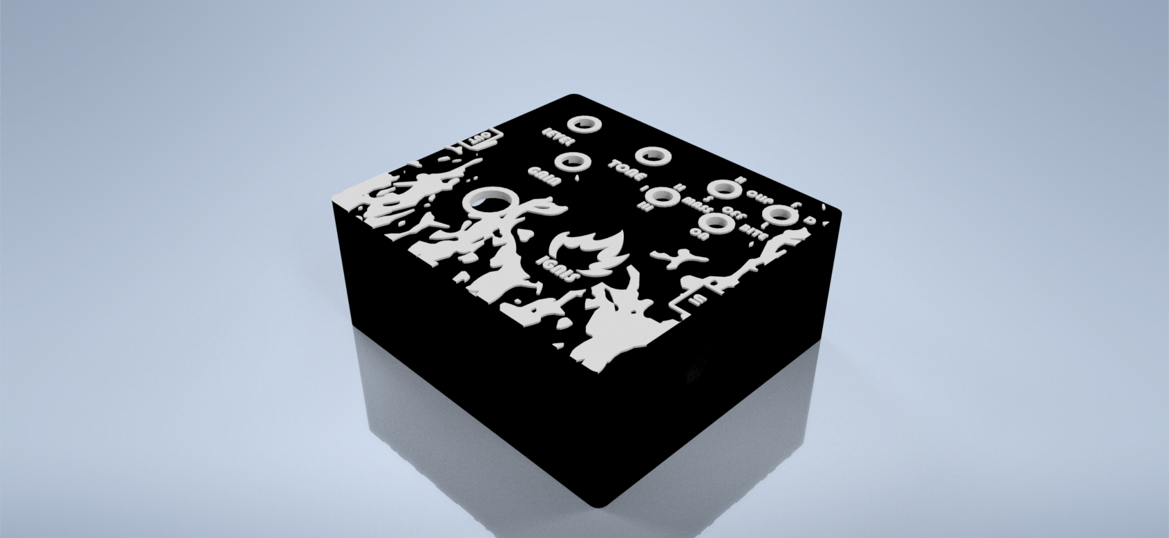
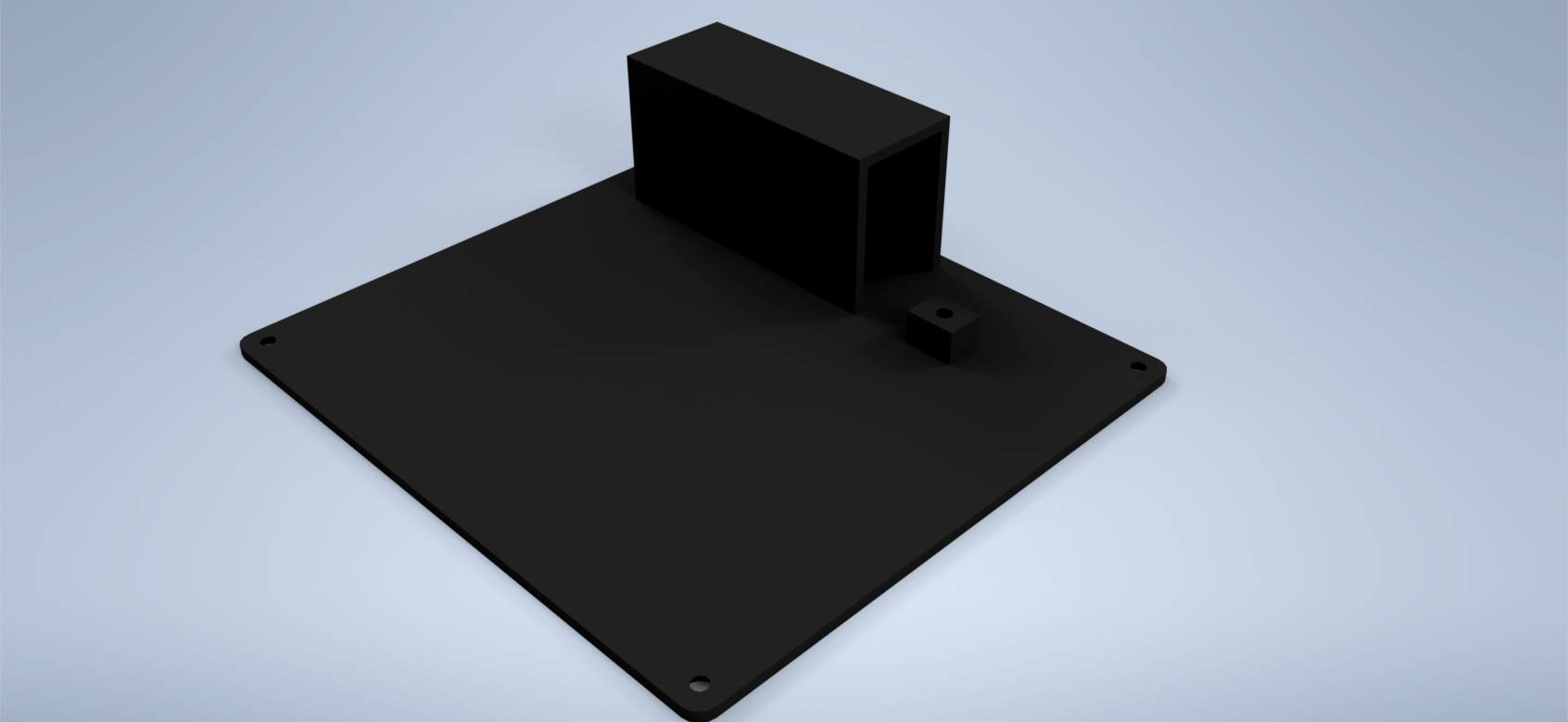
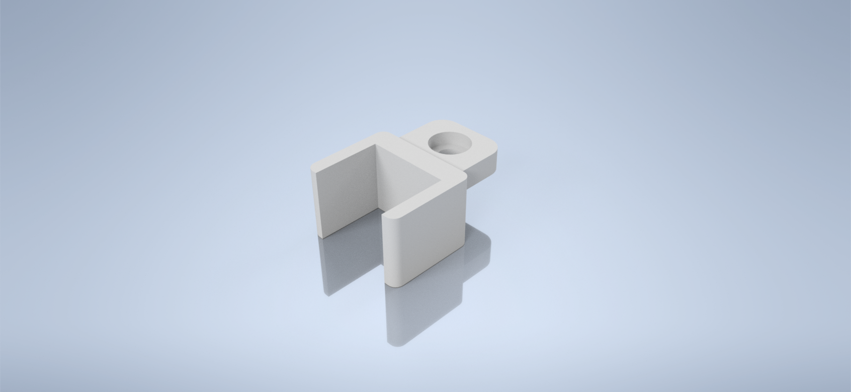
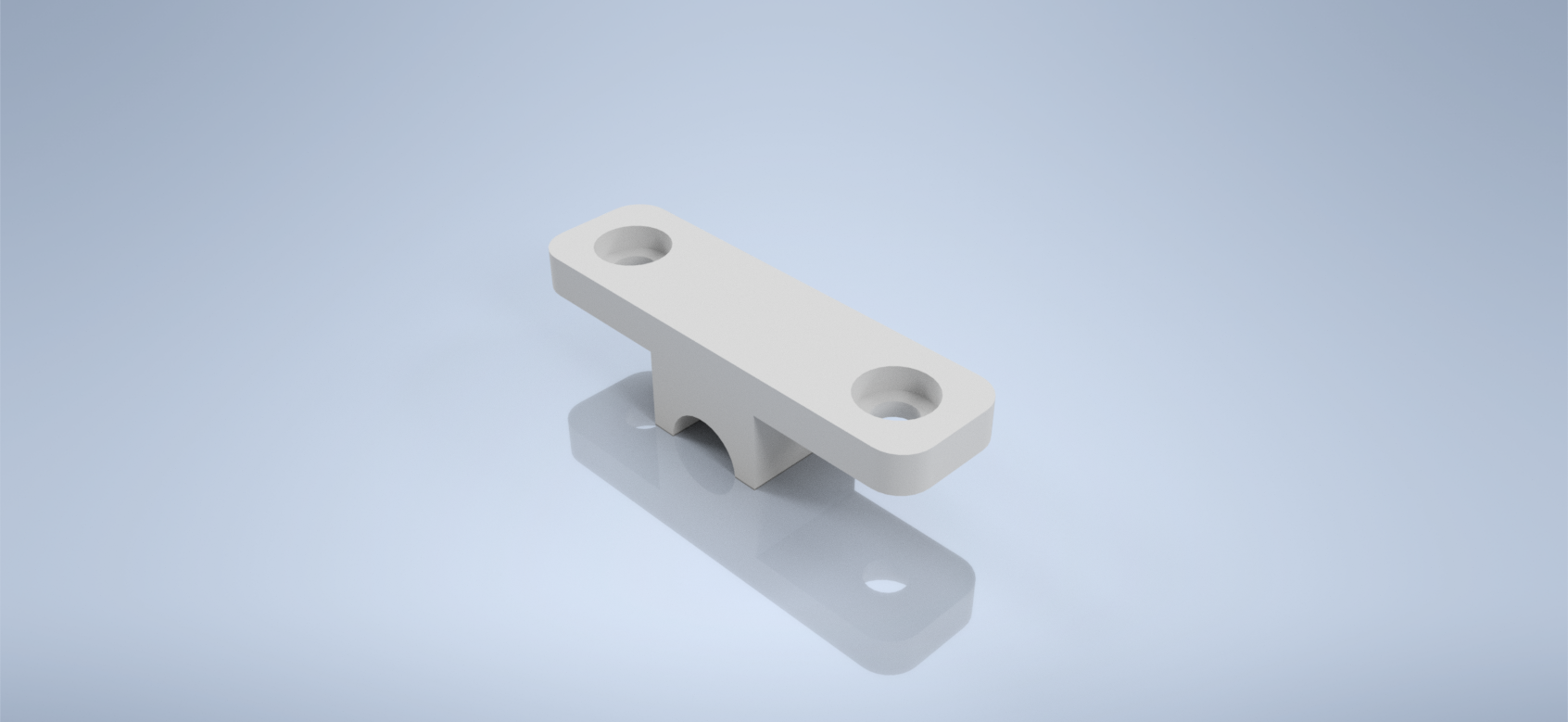
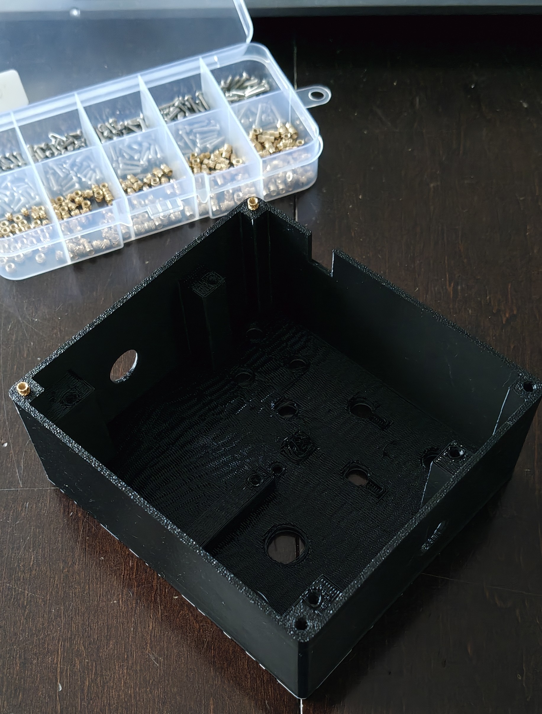
The project includes custom .stl files for a fully 3D-printable enclosure, designed from the ground up for mechanical reliability and easy assembly.
| Reference | Qty | Value | Description/Type |
|---|---|---|---|
| BT1 | 1 | Battery connector | Female 6F22 connector |
| C1,C2 | 2 | 47u | Electrolytic Capacitor THT 9V (Radial) |
| C3 | 1 | 470n | Ceramic/Electrolytic Capacitor THT 9V |
| C4 | 1 | 220n | Ceramic Capacitor THT 9V |
| C5,C9 | 2 | 1u | Electrolytic Capacitor THT 9V (Radial) |
| C6 | 1 | 2.2u | Electrolytic Capacitor THT 9V (Radial) |
| C7 | 1 | 100p | Ceramic Capacitor THT 9V |
| C8 | 1 | 22n | Ceramic Capacitor THT 9V |
| D1,D2 | 2 | 1N4148 | 1N4148 500mV |
| D3,D4 | 2 | LED | Red LED THT D3.0mm |
| D5 | 1 | LED | Red LED THT D5.0mm |
| FS1-9 | 1 | 3PDT | 3PDT Bistable Footswitch M12 |
| J3 | 1 | Barrel_Jack_Switch | Standard 5.5 mm x 2.1 mm female DC supply connector |
| Jack1,Jack2 | 2 | Audio Jack | Female barrel jack 6.35mm - Thomann SK096* |
| R1,R2,R6 | 3 | 10k | Standard THT (1/4W) |
| R3 | 1 | 1M | Standard THT (1/4W) |
| R4 | 1 | 100k | Standard THT (1/4W) |
| R5 | 1 | 1k | Standard THT (1/4W) |
| RV1 | 1 | 1M | Standard 16mm Rotary Potentiometer (with M7 Nut) |
| RV2,RV3 | 2 | 10k | Standard 16mm Rotary Potentiometer (with M7 Nut) |
| Knob | 3 | - | 15x17mm Plastic Knob |
| SW1, SW3 | 2 | - | MTS 102 (with M6 Nut) |
| SW2, SW4 | 2 | - | MTS 103 (with M6 Nut) |
| U1 | 1 | LM358 | Standard DIP-8 |
| PCB | 1 | - | Professionally or DIY manufactured (files) |
| enclosure | 1 | - | 3D PETG Print bicolor (files) |
| base | 1 | - | 3D PETG Print monocolor (files) |
| LED holder | 1 | - | 3D PETG Print monocolor (files) |
| M2 insert | 9 | - | M2x4mm |
| M2 screw | 9 | - | M2x6mm |
| wire | >5.5m | - | AWG 22 |
| heatshrink | 60cm | - | <2mm |
| WAGO connector | 2 | - | WAGO 221-412* |
*- it can be easily replaced by similar element
[!NOTE] Note: The total estimated cost of manufacturing this project (including all electronic components, PCB fabrication, and 3D printing materials) is around
$28/€24, offering boutique-level versatility at a fraction of the retail price.
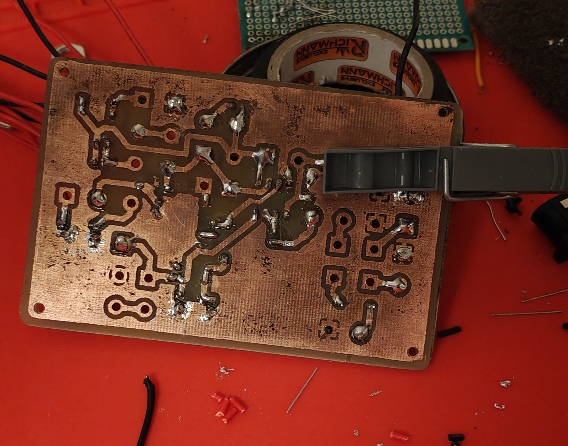
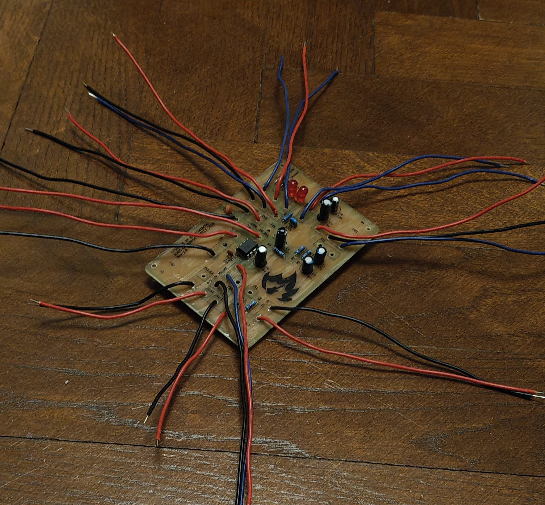
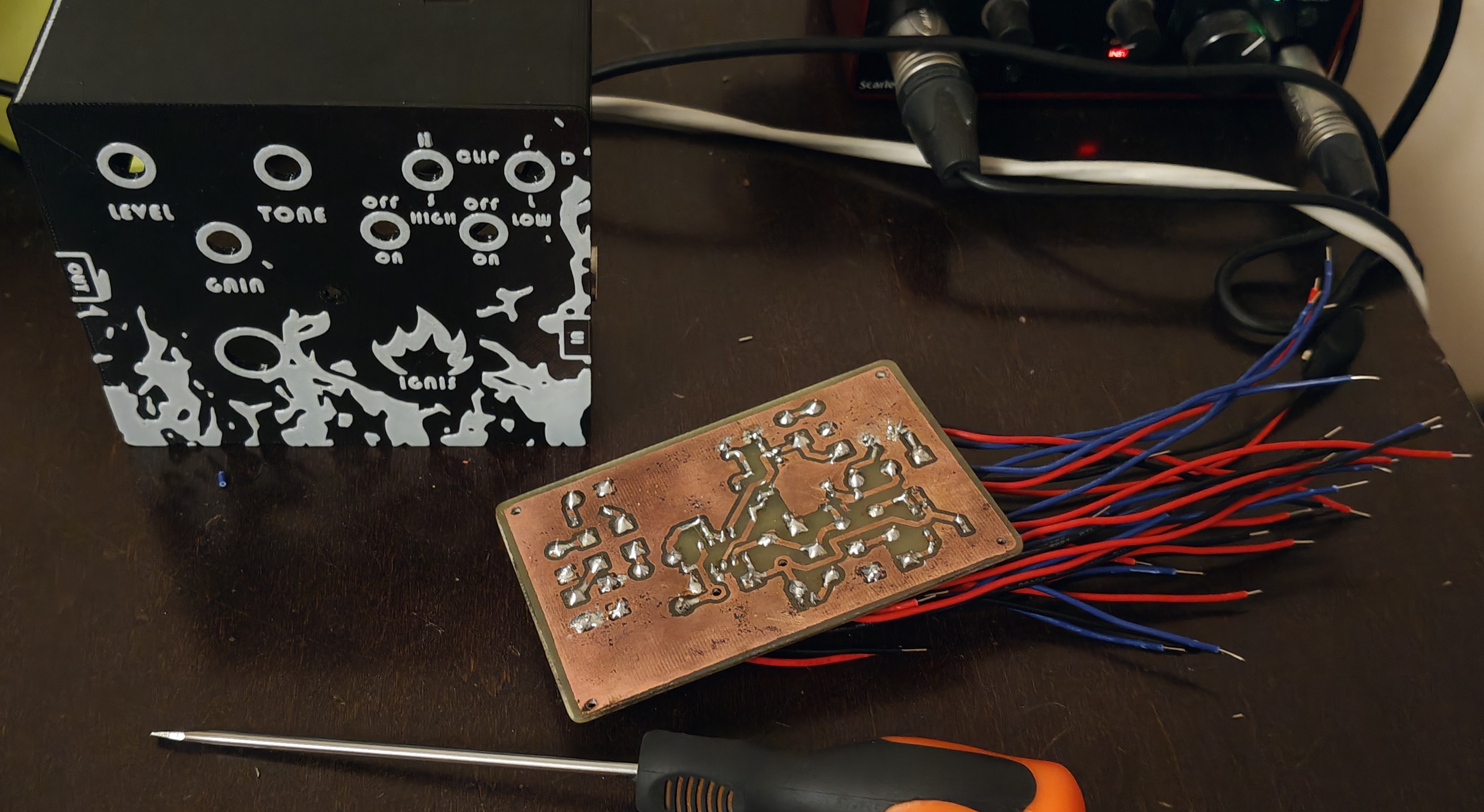
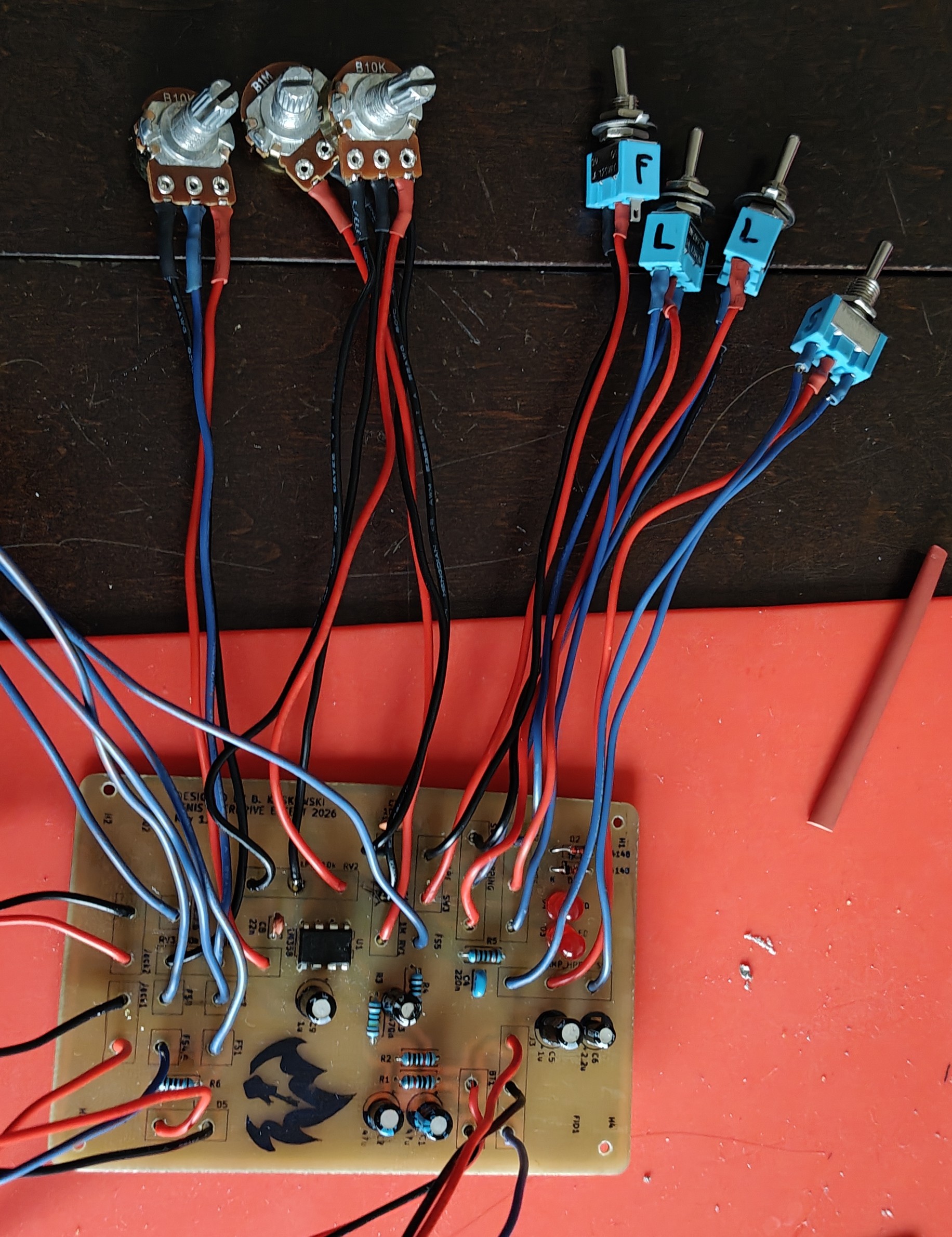
Shield: 
This work is licensed under a Creative Commons Attribution-NonCommercial 4.0 International License.

| Qty | Value | Footprint | References |
|---|---|---|---|
| 4 | MountingHole_Pad | MountingHole:MountingHole_2.7mm_M2.5_DIN965_Pad | H1, H2, H3, H4 |
| 3 | 10k | Resistor_THT:R_Axial_DIN0207_L6.3mm_D2.5mm_P7.62mm_Horizontal | R1, R2, R6 |
| 3 | Fiducial | Fiducial:Fiducial_1.5mm_Mask3mm | FID1, FID2, FID3 |
| 2 | 10k | Connector_Wire:SolderWire-1sqmm_1x03_P7.8mm_D1.4mm_OD3.9mm | RV2, RV3 |
| 2 | 1N4148 | Diode_THT:D_DO-35_SOD27_P7.62mm_Horizontal | D1, D2 |
| 2 | 1u | Capacitor_THT:CP_Radial_D6.3mm_P2.50mm | C5, C9 |
| 2 | 47u | Capacitor_THT:CP_Radial_D6.3mm_P2.50mm | C1, C2 |
| 2 | Audio Jack | Connector_Wire:SolderWire-1sqmm_1x02_P7.8mm_D1.4mm_OD3.9mm | Jack1, Jack2 |
| 2 | LED | LED_THT:LED_D3.0mm | D3, D4 |
| 2 | LOGO | LOGO | G***, G*** |
| 2 | SW_SPDT_MSM | Connector_Wire:SolderWire-1sqmm_1x03_P7.8mm_D1.4mm_OD3.9mm | SW2, SW4 |
| 1 | 100k | Resistor_THT:R_Axial_DIN0207_L6.3mm_D2.5mm_P7.62mm_Horizontal | R4 |
| 1 | 100p | Capacitor_THT:C_Disc_D3.4mm_W2.1mm_P2.50mm | C7 |
| 1 | 1M | Resistor_THT:R_Axial_DIN0207_L6.3mm_D2.5mm_P7.62mm_Horizontal | R3 |
| 1 | 1M | Connector_Wire:SolderWire-1sqmm_1x03_P7.8mm_D1.4mm_OD3.9mm | RV1 |
| 1 | 1k | Resistor_THT:R_Axial_DIN0207_L6.3mm_D2.5mm_P7.62mm_Horizontal | R5 |
| 1 | 2,2u | Capacitor_THT:CP_Radial_D6.3mm_P2.50mm | C6 |
| 1 | 220n | Capacitor_THT:C_Disc_D3.4mm_W2.1mm_P2.50mm | C4 |
| 1 | 22n | Capacitor_THT:C_Disc_D3.4mm_W2.1mm_P2.50mm | C8 |
| 1 | 3PDT P1 | Connector_Wire:SolderWire-1sqmm_1x01_D1.4mm_OD3.9mm | FS1 |
| 1 | 3PDT P2,3,6 | Connector_Wire:SolderWire-1sqmm_1x01_D1.4mm_OD3.9mm | FS2,3,6 |
| 1 | 3PDT P4,9 | Connector_Wire:SolderWire-1sqmm_1x01_D1.4mm_OD3.9mm | FS4,9 |
| 1 | 3PDT P5 | Connector_Wire:SolderWire-1sqmm_1x01_D1.4mm_OD3.9mm | FS5 |
| 1 | 3PDT P7 | Connector_Wire:SolderWire-1sqmm_1x01_D1.4mm_OD3.9mm | FS7 |
| 1 | 3PDT P8 | Connector_Wire:SolderWire-1sqmm_1x01_D1.4mm_OD3.9mm | FS8 |
| 1 | 470n | Capacitor_THT:C_Disc_D3.4mm_W2.1mm_P2.50mm | C3 |
| 1 | Barrel_Jack_Switch | Connector_Wire:SolderWire-1sqmm_1x03_P7.8mm_D1.4mm_OD3.9mm | J3 |
| 1 | Battery | Connector_Wire:SolderWire-1sqmm_1x02_P7.8mm_D1.4mm_OD3.9mm | BT1 |
| 1 | LED | Connector_Wire:SolderWire-1sqmm_1x02_P7.8mm_D1.4mm_OD3.9mm | D5 |
| 1 | LM358 | Package_DIP:DIP-8_W7.62mm_LongPads | U1 |
| 1 | SW_Nidec_CAS-120A1 | Connector_Wire:SolderWire-1sqmm_1x03_P7.8mm_D1.4mm_OD3.9mm | SW1 |
| 1 | SW_SPST | Connector_Wire:SolderWire-1sqmm_1x02_P7.8mm_D1.4mm_OD3.9mm | SW3 |
peterheinrich/InternetOverSpaghetti
Transmitting IP packages over a pair of spaghetti thus demonstrating how media independent IP really is.

zmaker/arduino_cookbook
gli sketch del nuovo progetto Arduino Cookbook e dei video di YouTube

profdc9/RFBitBanger
A QRP digital transceiver created from readily available parts for off-the-grid maintenance


tvlad1234/pillScopePlus
Oscilloscope based around the STM32F401 Black Pill and a color LCD screen


starlightk7/OpenSFC
OSHW Reproduction Parts related to the Super Famicom / Super Nintendo game console

It measures 65 × 99 mm and has 2 copper layers, 1.6 mm thick.
47 parts, built around the LM358. The full list of its parts is on this page, with links to each part's symbol and footprint where PCBKit's library has them.
From the Quee0/Ignis-overdrive repository on GitHub, at the commit this page was made from: the board is overdrive_effect/overdrive_effect.kicad_pcb and its schematic overdrive_effect/overdrive_effect.kicad_sch. PCBKit opens the board in the browser, with nothing to install.
Its repository states no licence, so its author keeps all rights: ask Quee0 before reusing the design.