Class-D Stereo Amplifier PCB





A stereo Class-D audio amplifier PCB built around the TPA3116D2, designed to deliver efficient and high-power audio output from a 24V supply. The board integrates a complete signal chain from analog input to filtered speaker output, while maintaining a compact and practical layout suitable for real-world applications.
Preview
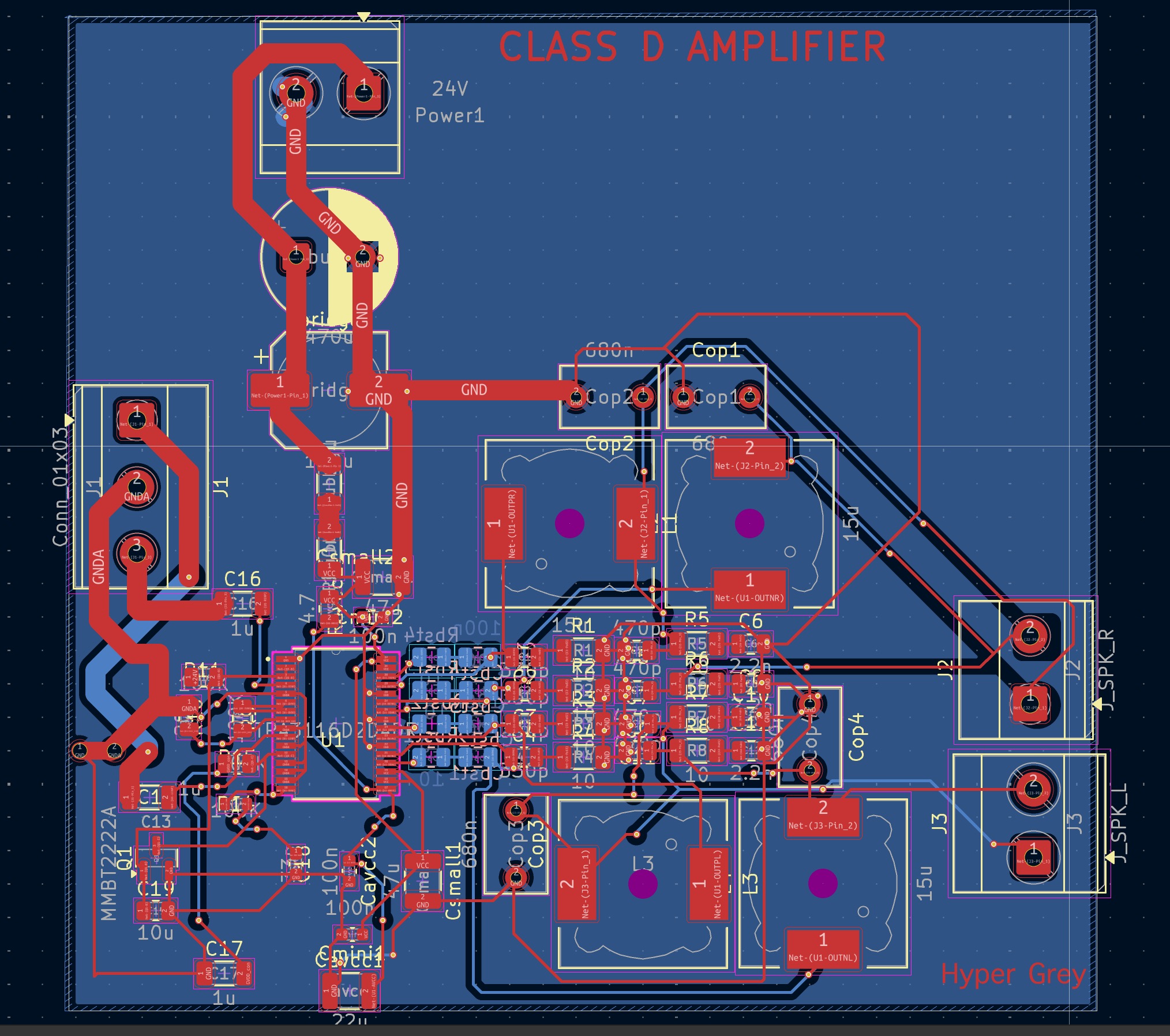
PCB Layout
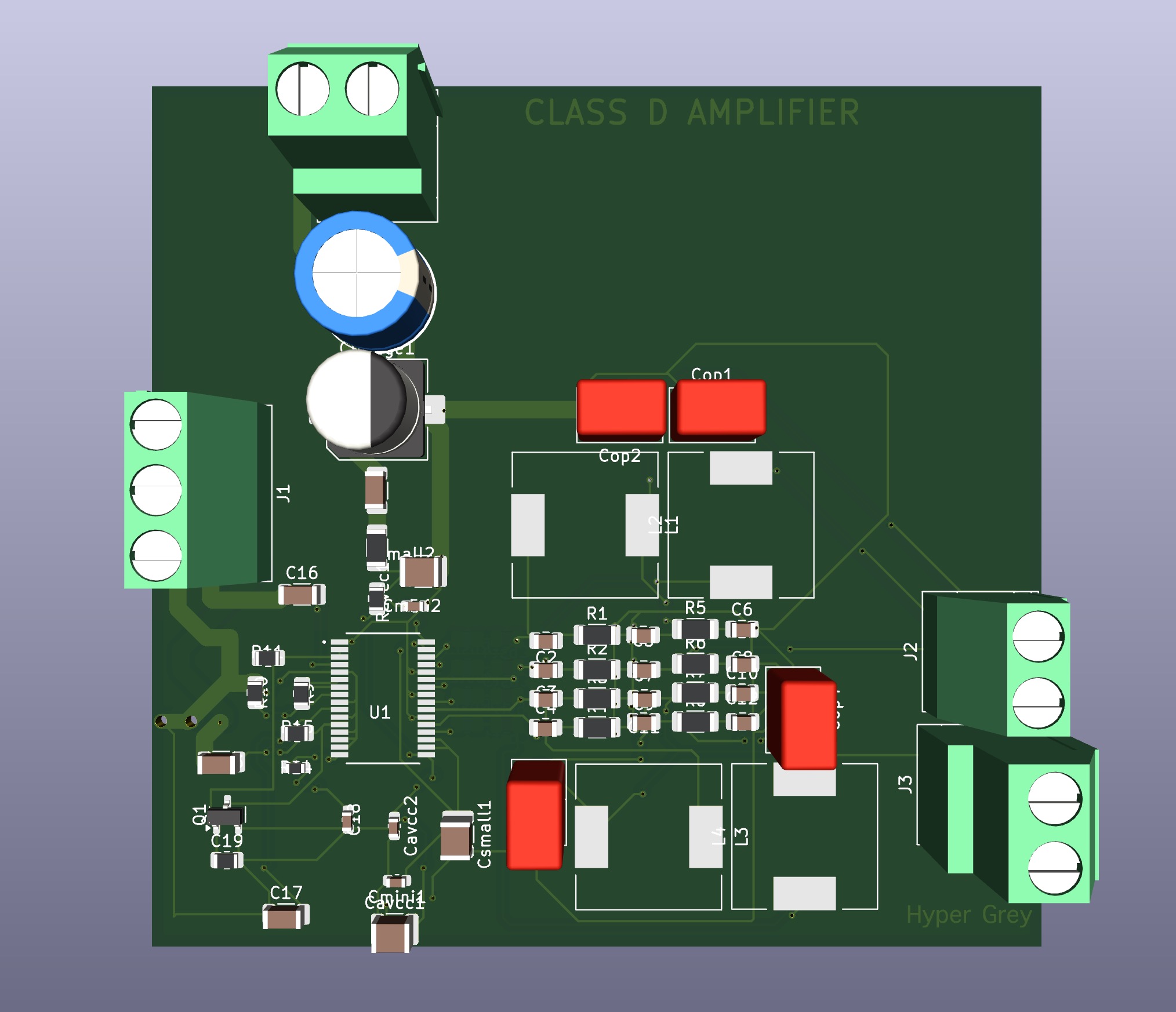
3D View
Features
- Stereo audio amplifier (Left and Right channels)
- 24V power input design
- Based on TPA3116D2 Class-D amplifier IC
- LC low-pass filters for output signal smoothing
- RC snubber networks for switching noise suppression
- Screw terminal connectors for power and speakers
- Ground plane implementation for improved performance
- Compact and structured component placement
Design Overview
Signal Chain
- Audio input via 3-pin connector (L, R, GND)
- Input conditioning network
- Amplification using TPA3116D2
- LC filtering stage for each channel
- Output to speaker terminals
Power Design
- 24V input with bulk capacitor filtering
- Local decoupling capacitors placed near IC
- Wide traces for high-current paths
PCB Design Highlights
- Bottom-layer ground plane to reduce impedance and improve return paths
- Multiple vias connecting IC ground and decoupling capacitors to ground plane
- Wide traces for power and output routing
- Separation between high-frequency switching nodes and low-level signals
- LC filters placed close to output stage to minimize noise
- Logical component placement based on signal flow
Project Structure
hardware/
├── ClassD_Amplifier.kicad_sch
├── ClassD_Amplifier.kicad_pcb
└── ClassD_Amplifier.kicad_pro
Images/
├── pcb.png
├── pcb_3d.png
└── schematic.png
Learning Goals
- Understanding Class-D amplifier operation
- Designing LC filters for switching systems
- PCB layout for power electronics
- Grounding and return path optimization
- Managing noise and EMI in mixed-signal designs
Tools Used
- KiCad (Schematic and PCB design)
- KiCad 3D Viewer
- Datasheet-driven design approach
Challenges
- Managing switching noise and EMI
- Routing high-current traces efficiently
- Maintaining clean grounding
- Avoiding interference between power and signal sections
Future Improvements
- Add mounting holes
- Improve silkscreen clarity
- Optimize trace routing further
- Thermal considerations and heat management
- Better isolation between signal and power sections
Notes
This project is intended as a practical learning exercise in audio and power PCB designing


