

2 layers58 × 37.1 mm
Phils Lab #165
ctrl-z3d/pcb-designs
A personal archive of PCB projects I've designed and built along the way. Schematics, board layouts, manufacturing files, and notes.
37 parts1

 Naveens-Lab/mspm0g3507-evm
EVM-style dev board — TI MSPM0G3507 + ATECC608A secure element | KiCad 9.0 | REV A
MSPM0 DevBoard is an open-source printed circuit board by Naveens-Lab, from the Naveens-Lab/mspm0g3507-evm repository on GitHub. It is a 2-layer board of 56 × 34.3 mm with 38 parts on 65 nets, routed with 262 tracks and 36 vias.
It is built around the MSPM0G3507SPTR, CH340E and ATECC608A-SSHDA-T, with the SPX3819M5-L-3-3, USBLC6-2SC6 and CL21B474KBFNNNE among its other parts. Its parts include 14 capacitors, 8 resistors, 5 ICs, 2 connectors and 1 crystal. It belongs with the microcontroller boards boards of this library.


An embedded software engineer's journey into hardware design.




A custom EVM (Evaluation Module) style development board built around the TI MSPM0G3507 microcontroller. The project started as a personal deep-dive into schematic and PCB design something I had always wanted to do coming from an embedded software background and has grown into a platform I intend to keep expanding.
The board includes a Microchip ATECC608A hardware secure element, making it suitable for exploring hardware-backed cryptography, device authentication, and secure key storage on a board I designed myself. Beyond the learning aspect, I plan to build real applications here: IoT device authentication, secure bootloader prototyping, and more.
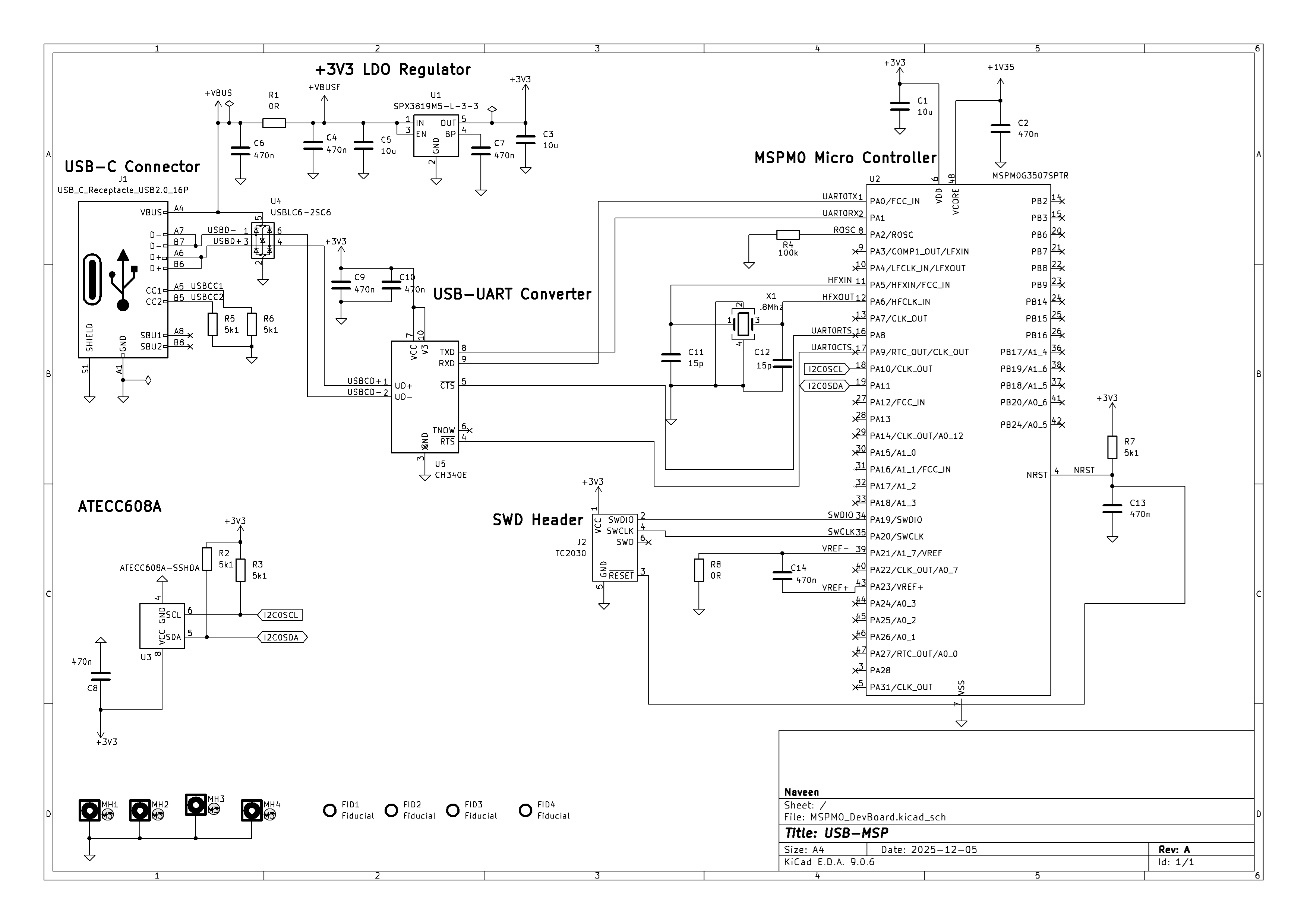
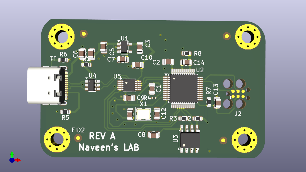
| Ref | Part | Description |
|---|---|---|
| U2 | TI MSPM0G3507SPTR | 32-bit Arm Cortex-M0+, 80MHz, 128KB Flash, LQFP-64 |
| U3 | Microchip ATECC608A-SSHDA | Hardware secure element — ECC, SHA-256, I2C interface |
| U1 | SPX3819M5-L-3-3 | 3.3V LDO voltage regulator |
| U4 | USBLC6-2SC6 | USB line ESD protection (bidirectional TVS) |
| U5 | CH340E | USB-to-UART bridge IC |
| J1 | USB-C Receptacle | USB 2.0, 16P — power input + UART comms |
| J2 | TC2030 (Tag-Connect) | SWD debug/programming header — no connector bulk |
| X1 | 8 MHz Crystal | High-frequency external oscillator (HFXT) |
| R2, R3 | 5.1kΩ | I2C pull-ups for ATECC608A (SCL / SDA) |
| R5, R6 | 5.1kΩ | USB-C CC1 / CC2 pull-downs (UFP/sink mode) |
                    +3V3
                     │
  USB-C ─► USBLC6 ─► CH340E ──(UART0: PA0/PA1)──► MSPM0G3507SPTR
                              │                         │
                       UD+/UD-│                    I2C0 (PA10/PA11)
                              │                         │
                         (USB FS)                  ATECC608A-SSHDA
                                                   (Secure Element)

  SWD ─► TC2030 ──(SWDIO: PA19 / SWCLK: PA20)──► MSPM0G3507SPTR

VBUS ─► SPX3819M5-L-3-3 (LDO) ─► +3V3 (board rail)mspm0g3507-evm/
├── assets/
│ ├── schematic.png # Schematic export
│ └── pcb_3d_top.png # PCB 3D render — REV A
├── kicad/
│ ├── MSPM0_DevBoard.kicad_pro
│ ├── MSPM0_DevBoard.kicad_sch
│ ├── MSPM0_DevBoard.kicad_pcb
│ └── MSPM0G3507_Sym_Symbl.kicad_sym # Custom MCU symbol library
├── datasheets/ # MSPM0G3507, ATECC608A, CH340E, SPX3819
├── gerbers/ # Generated at fab-ready milestone
├── firmware/ # Bring-up and demo firmware
└── README.mdI have spent 6+ years as an embedded software engineer writing firmware for automotive EV , elevator controllers, medical devices, and defense systems. I have always worked on top of hardware that someone else designed. This project is me crossing that line: learning how the schematic becomes a PCB, how a PCB becomes a product, and how every decision made during layout shows up as a bug (or not) at bring-up.
The ATECC608A is here because hardware-backed security is something I want to understand deeply not just at the register level from firmware, but from the moment the footprint lands on the board.
This is REV A. It will not be perfect. That is the point.
Hardware design files (schematic, PCB) licensed under CERN Open Hardware Licence v2 - Permissive (CERN-OHL-P).
Firmware licensed under MIT.
Naveen — Embedded Systems Engineer
Firmware architecture ·Hardware-firmware integration
Automotive · Industrial · Power Electronics
| Qty | Value | Footprint | References |
|---|---|---|---|
| 9 | 470n | Capacitor_SMD:C_0805_2012Metric | C2, C4, C6, C7, C8, C9, C10, C13, C14 |
| 5 | 5k1 | Resistor_SMD:R_0603_1608Metric | R2, R3, R5, R6, R7 |
| 4 | Fiducial | Fiducial:Fiducial_1mm_Mask2mm | FID1, FID2, FID3, FID4 |
| 4 | M3 | MountingHole:MountingHole_3.2mm_M3_Pad_Via | MH1, MH2, MH3, MH4 |
| 3 | 10u | Capacitor_SMD:C_0805_2012Metric | C1, C3, C5 |
| 2 | 0R | Resistor_SMD:R_0603_1608Metric | R1, R8 |
| 2 | 15p | Capacitor_SMD:C_0805_2012Metric | C11, C12 |
| 1 | .8Mhz | Crystal:Crystal_SMD_3225-4Pin_3.2x2.5mm | X1 |
| 1 | 100k | Resistor_SMD:R_0201_0603Metric | R4 |
| 1 | ATECC608A-SSHDA | Package_SO:SOIC-8_3.9x4.9mm_P1.27mm | U3 |
| 1 | CH340E | Package_SO:MSOP-10_3x3mm_P0.5mm | U5 |
| 1 | MSPM0G3507SPTR | Package_QFP:LQFP-48_7x7mm_P0.5mm | U2 |
| 1 | SPX3819M5-L-3-3 | Package_TO_SOT_SMD:SOT-23-5 | U1 |
| 1 | TC2030 | Connector:Tag-Connect_TC2030-IDC-FP_2x03_P1.27mm_Vertical | J2 |
| 1 | USBLC6-2SC6 | Package_TO_SOT_SMD:SOT-23-6 | U4 |
| 1 | USB_C_Receptacle_USB2.0_16P | Connector_USB:USB_C_Receptacle_GCT_USB4105-xx-A_16P_TopMnt_Horizontal | J1 |
ctrl-z3d/pcb-designs
A personal archive of PCB projects I've designed and built along the way. Schematics, board layouts, manufacturing files, and notes.

hykoser/LIS2DH-Accelerometer-Board
A custom accelerometer development board designed with KiCad and MSPM0 microcontroller.

prashantbhandary/mspmo-baord
A compact USB-C development board for TI's MSPM0G3507 (Arm Cortex-M0+, 80 MHz, 128 KB flash, 32 KB SRAM), with an on-board USB-to-UART bridge, a 3-axis accelerometer and a Tag-Connect SWD footprint.

adityajoshi2008/MSPM0-DevKit
🌐 ARM Cortex-M0+ • KiCad 10.0 • Open Source • PCB Hardware

akshat-kumar10/MSMP0_PCB
A PCB for an MSMP0 board that features a Modbus Transceiver & Analog Front-End (AFE) for Sensors


basillx1/mspm0-accelerometer-board
2-layer KiCad board: TI MSPM0 MCU + LIS2DH accelerometer, USB-C, SWD debug

benbruder/MSPM0
Design of schematic and PCB for a TI MSPM0-based MCU with all of its components.
It measures 56 × 34.3 mm and has 2 copper layers, 1.6 mm thick.
38 parts, built around the MSPM0G3507SPTR, CH340E, ATECC608A-SSHDA-T and SPX3819M5-L-3-3. The full list of its parts is on this page, with links to each part's symbol and footprint where PCBKit's library has them.
From the Naveens-Lab/mspm0g3507-evm repository on GitHub, at the commit this page was made from: the board is MSPM0_DevBoard.kicad_pcb and its schematic MSPM0_DevBoard.kicad_sch. PCBKit opens the board in the browser, with nothing to install.
Its repository states no licence, so its author keeps all rights: ask Naveens-Lab before reusing the design.