
2 layers297.2 × 180.3 mm

 Mikejmoffitt/md-opn2c3
Adapter for OPN2C (YM3438) use on Megadrive in place of OPN2 (YM2612).
Md opn2c is an open-source printed circuit board by Mikejmoffitt, from the Mikejmoffitt/md-opn2c repository on GitHub. It is a 2-layer board of 48.7 × 23.9 mm with 50 parts on 57 nets, routed with 328 tracks and 57 vias.
It is built around the 74HCT08D. Its parts include 20 resistors, 13 capacitors, 3 ICs and 2 connectors. It belongs with the interfaces and adapters boards of this library.
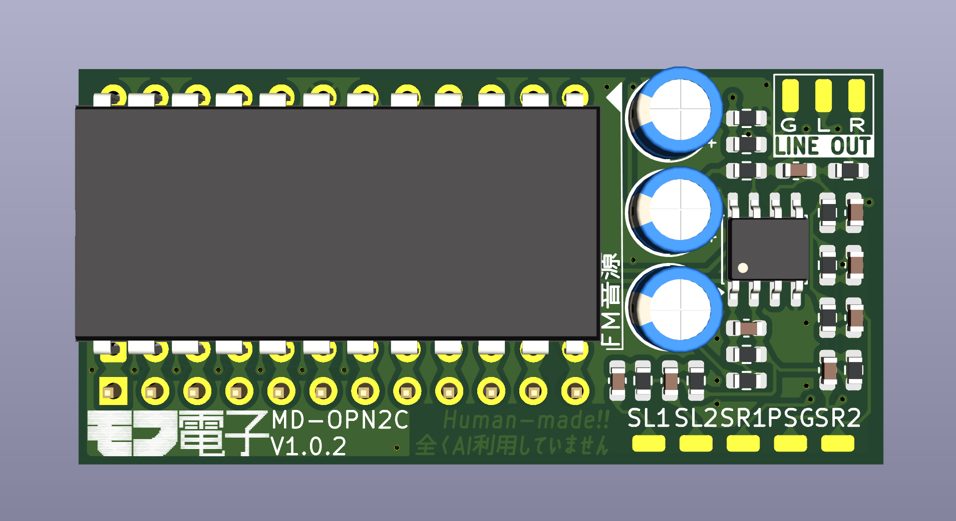
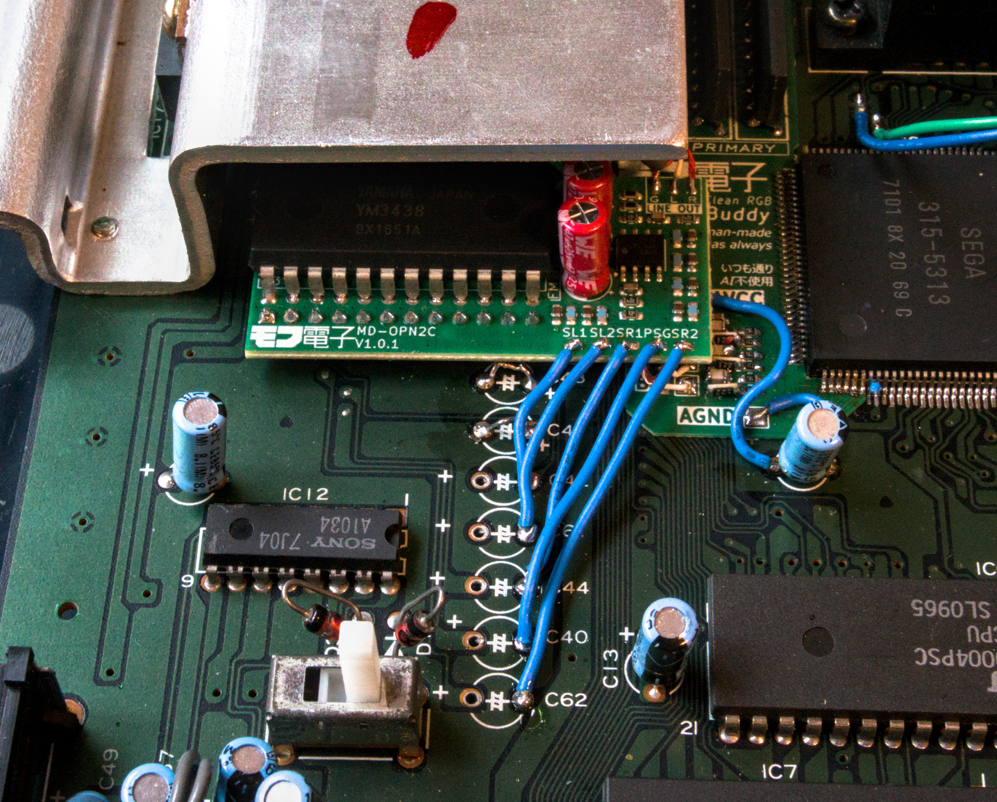
このアダプターでメガドライブ初代はYM3438(OPN2C)が対応できるようになります。 元々の音源のステータスレジスターの読み込みの違いを解決するとジックがついています。 その上オープンソースのトリップルバイパス)より綺麗な音源のミクサーとバッファーがついていて、元々のヘッドホンも専用ライン出力が使えるようになります。
元々のFM音源(YM2612)を抜いて使用することも可能です。 その場合は3BPと同じような使い方になります。 その場合でもヘッドホンもラインアウトも利用できます。
メガドラVA0の基板を参考しながら書いたんですが、基本的にすべての初代の基板は互換はずです。
This adapter facilitates the install of a YM3438 (OPN2C) in a Sega Mega Drive or Genesis console. Glue logic is present to solve status read bugs that invoke different behavior between the original YM2612 and the CMOS YM3438. In addition, a mixing and buffering circuit (courtesy of the open source Triple Bypass PCB) to both handle the new YM3438 and also provide clean mixing for other signals. The buffer circuit also has provisions to output audio to the original signal path, so that the mono audio output and the headphone jack both work as designed.
An original YM2612 may also be installed, in which case this PCB simply provides a new mixing circuit and buffer, similar to the Triple Bypass PCB).
These instructions were written using a Japanese VA0 unit as a reference, but principally can apply to any Megadrive or Genesis with a YM2612 in it.
メガドライブ(初代)VA0-VA6は互換です。 ジェネシス2のVA3でも動くかもしれませんが、未確認なので一応保証ができません。 Compatible with Genesis 1 / Megadrive 1 VA0-VA6. Genesis 2 VA3 (with discrete YM2612) may work, but has not been tested, and I cannot provide installation instructions at this time.
マザーに付ける前に修正が必要です.
With the adapter unit ready, some work must be done to the Megadrive motherboard.
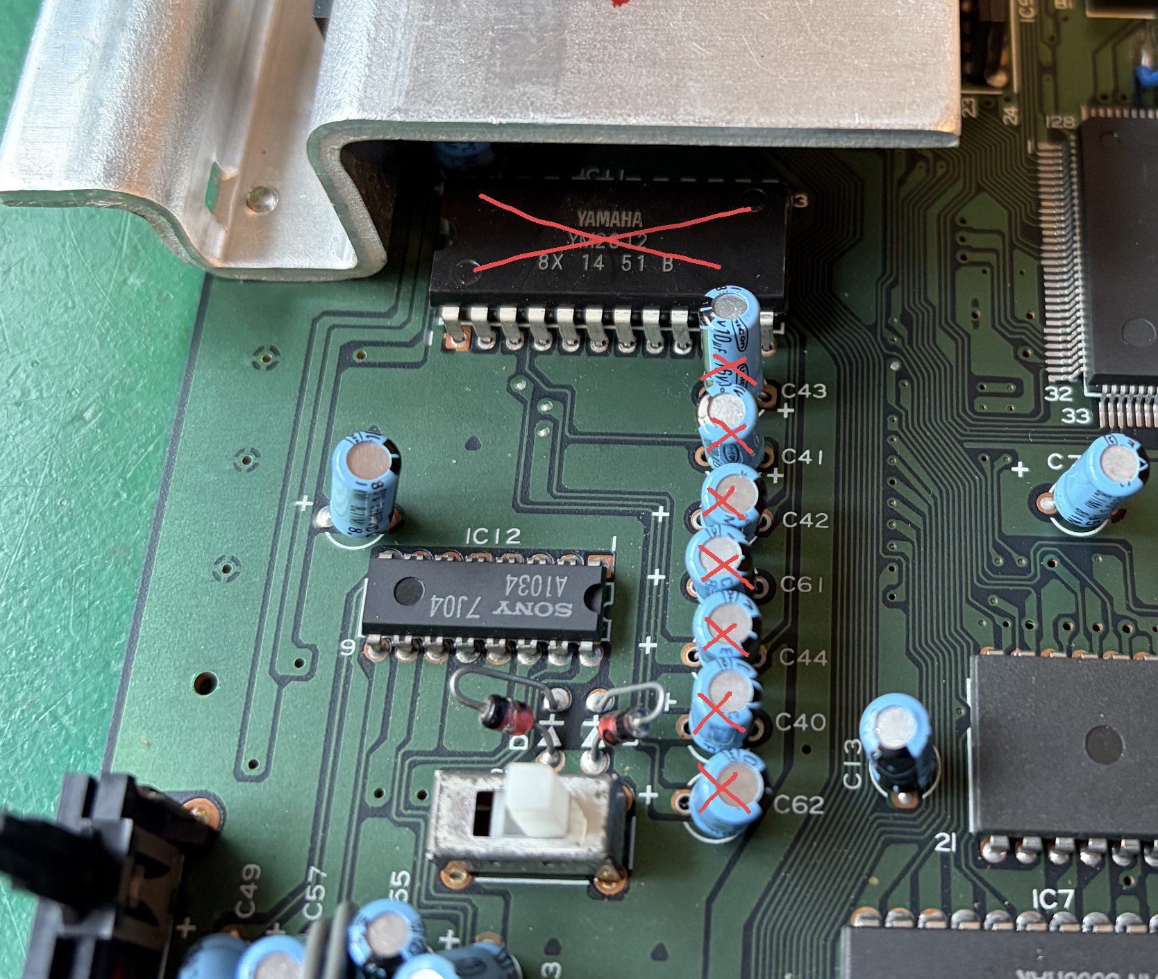
YM2612を外して、どこか保存しします。(依頼要らないけど捨てないでください!) 下の縦列のコンデンサーも外しましょう。(C40, C41, C42, C43, C44, C61, C62)
Desolder and remove the YM2612, and the column of capacitors below it (C40, C41, C42, C43, C44, C61, and C62).
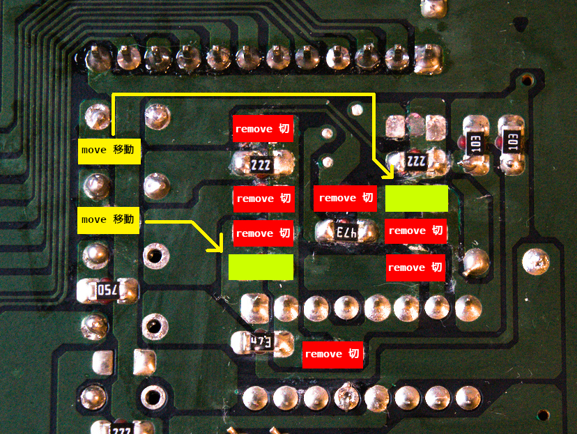
底面に赤く示している部品を外します。 (R34, R37, R40, R41, C45, C46, C47, C48)。 左の黄色いやつを外して、右の緑の部品に移動します。 (R53/R43, R40/R41)。 C41とC43の穴にリンクを入れてください。
下面に印刷がないので下の絵を参考してください。
On the underside, remove the components marked in red (R34, R37, R40, R41, C45, C46, C47, C48). Remove the components marked in yellow (R53 and R43) and move them to the spot marked in green (R40 and R41). Install a link between the two pins of capacitors C41 and C43.
As there is no silkscreen on the underside of most revisions, the diagram will be a helpful reference.
新しいミックスされた音声は元々のFM音源の端子に入ります(21ピンと20ピン)。 そのために元々のヘッドホンもモノの出力が使えます。
The new audio will enter through what used to be the MOL and MOR pins for the OPN2, at pins 21 and 20 respectively. The mixed stereo signals enter the original mixing circuit alone, where it then enters the headphone amp as well as the mono mixdown for the CXA-1145.
YM3438か先抜いたYM2612をアダプターの上面に付けます。 下面にピンが邪魔になってしまうので上面にハンダ付けても大丈夫です。 音源のICは完全に平にならないんですが、全ての端子がちゃんとついていたら問題がありません (少距離は大丈夫です)。
アダプターのウラ面にジャンパーがあります。 音源の種類によって左側か右側を半田で閉めて下さい。 両方のジャンパーを同じ設置するようにご注意下さい。
Attach either a YM3438 or the previously removed YM2612 in the open position on the adapter PCB. As the header pins on the underside may obstruct your soldering, it is fine to apply solder on the top side. The IC may not lay perfectly flat, but if all pins are firmly soldered a slight distance is acceptable.
On the underside of the adapter, use solder to close the jumpers based on the sound source type. You must set both sets of jumpers in the same configuration.
| 設定Config | IC類Chip |
|---|---|
(--- ) | YM2612 |
( ---) | YM3438 |
YM2612の場合は、音源の20/21ピンからグラウンド(19ピン)に2.2k抵抗器を付けて下さい。 次の改正に修正しますが、とりあえずこの小さい改造が必要になります。
In the case of a YM2612, attach two 2.2k resistors between pins 20/21 and ground (pin 19), as the YM2612 requires pulldown resistors. Pads for this will be incorporated in a future revision.
先の準備を完全似できたか確認しておいてください。
Please be sure you have completed the Motherboard Preparation steps first.
YM2612の位置にYM3438のアダプターを入れて、下面にハンダ付けます。 上面に5本の配線が必要です。 下の表を参考して
Place the assembled YM3438 adapter unit in the position that once held the original YM2612, and solder it in place on the underside. On the top, five wires are necessary to feed in the various audio signals that compliment the FM sound source. The table below describes the positions shown in the annotated picture below.
| 信号Signal | 出所Location |
|---|---|
| SL1 | C42 (-) |
| SL2 | C61 (-) |
| SR1 | C44 (-) |
| PSG | C40 (-) |
| SR2 | C62 (-) |
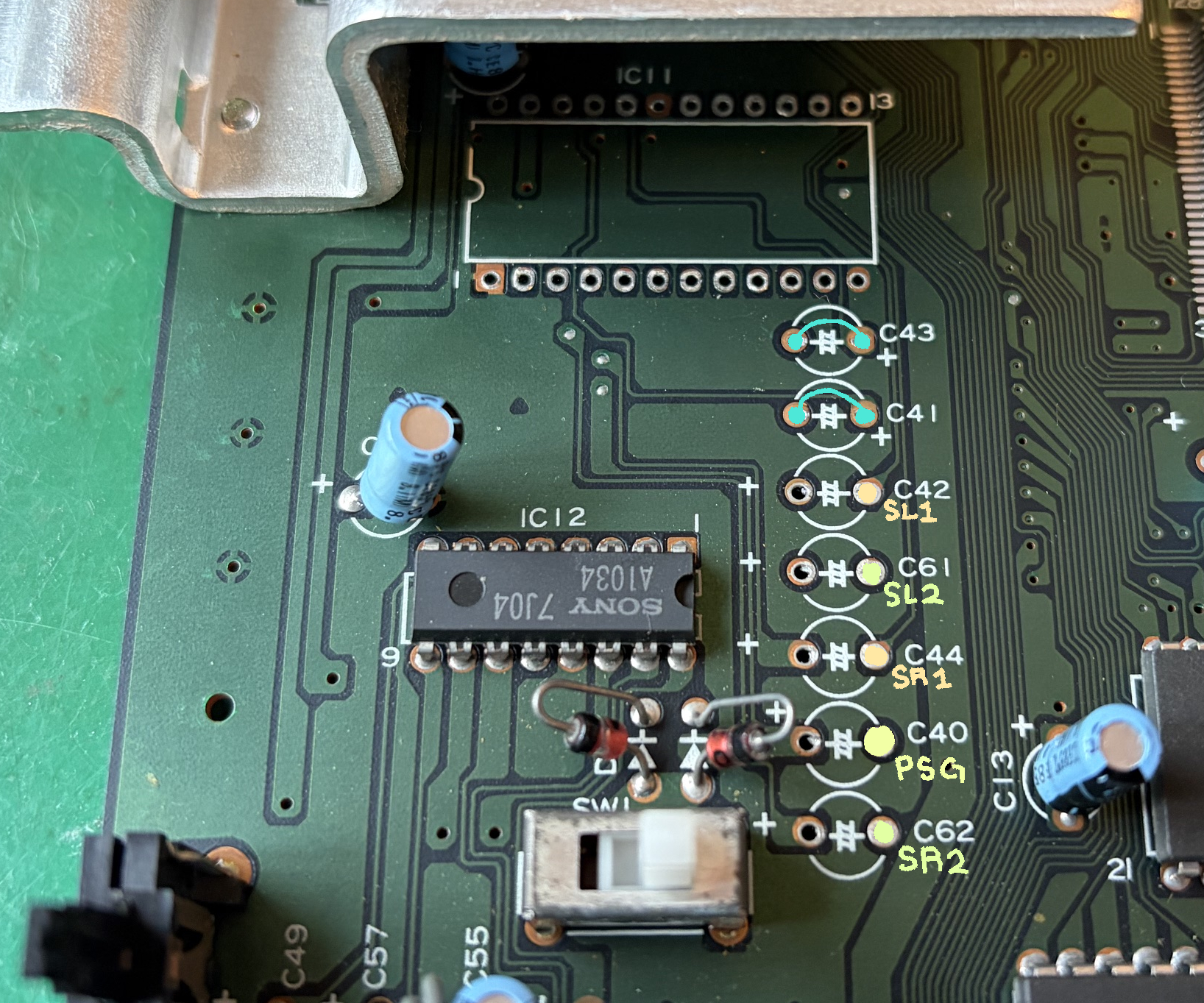
これで、どうやって出力を本体外に出すか自分の決まりです。 もしヘッドホンの端子が十分でしたらここまでストップしても大丈夫です。 しかし、ヘッドホンのアンプより直接LINE出力したらノイズが少なくなるので、LINEの出力はおすすめです。
アダプターにOUTのパッドがあります。 そこに配線付けて端子に繋げたらLINEの出力が可能です。
With everything installed, it's up to you how you want to route the audio out. If the headphone jack alone is adequate, you may stop here. However, I recommend a dedicated line out connection, as the headphone amp does introduce some noise.
The 'LINE OUT' pads are present so you may run a stereo output to the back of the console, or to some other connector of your choosing. Stereo audio will be present via the headphone jack, and mono audio will be delivered out of the rear A/V connector.
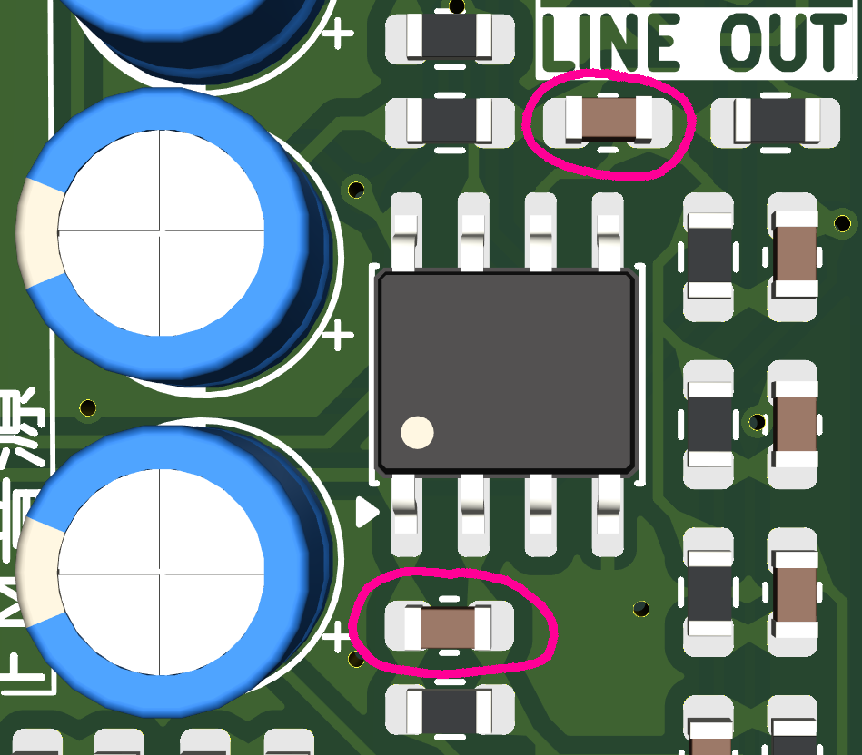
アダプタのLPFフィルターの遮断周波数は約16KHzになっていますが、もしVA3みたいな3KHzは希望だったらコンデンサー交換通じて可能です。 示しているコンデンサーを150Pfに交換すると、LPFの遮断周波数~3KHzになります。 元々のは33pFです。
The filter situated on the adapter has a fairly high cutoff frequency of about 16KHz. Unlike the triple bypass PCB, there isn't a selection of filter parameters, but if a stronger filter that sounds similar to the VA3 is desired, you may exchange the two highlighted capacitors for 150pF units to achieve a ~3.5KHz cutoff. The originals are 33pF.
テスト用基板です。 YM2612対応パッドがなくてYM3438だけを確認しました。
This version was made for testing. Pads to cooperate with YM2612 were not considered, and the operation of YM3438 was confirmed with this.
初版です。
First release.
形関わらずYM2612用レジスターを追加シました。
Optional pull-down resistors for YM2612 compatibility were added.
| Qty | Value | Footprint | References |
|---|---|---|---|
| 8 | TestPoint_Small | Connector_Wire:SolderWirePad_1x01_SMD_1x2mm | IN_PSG1, IN_SL1, IN_SL2, IN_SR1, IN_SR2, OUT_GND1, OUT_L1, OUT_R1 |
| 6 | 1uF/16V | Capacitor_SMD:C_0603_1608Metric | C3, C4, C5, C6, C7, C8 |
| 6 | 210k | Resistor_SMD:R_0603_1608Metric | R10, R11, R12, R13, R14, R15 |
| 4 | 100k | Resistor_SMD:R_0603_1608Metric | R8, R9, R22, R23 |
| 4 | 10k | Resistor_SMD:R_0603_1608Metric | R20, R21, R24, R25 |
| 2 | 10uF/16V | Capacitor_SMD:C_0603_1608Metric | C1, C2 |
| 2 | 2.2k | Resistor_SMD:R_0805_2012Metric | R2, R3 |
| 2 | 300k | Resistor_SMD:R_0603_1608Metric | R16, R17 |
| 2 | 330 | Resistor_SMD:R_0603_1608Metric | R18, R19 |
| 2 | 33pF/50V | Capacitor_SMD:C_0603_1608Metric | C9, C10 |
| 2 | 47uF/50V | Capacitor_THT:CP_Radial_D5.0mm_P2.50mm | C12, C13 |
| 2 | Conn_01x12_Pin | Connector_PinHeader_2.54mm:PinHeader_1x12_P2.54mm_Vertical | J1, J2 |
| 2 | SolderJumper_2_Open | Jumper:SolderJumper-2_P1.3mm_Open_TrianglePad1.0x1.5mm | JP3, JP4 |
| 2 | SolderJumper_3_Open | Jumper:SolderJumper-3_P2.0mm_Open_TrianglePad1.0x1.5mm | JP1, JP2 |
| 1 | 10uF/16V | Capacitor_THT:CP_Radial_D5.0mm_P2.50mm | C11 |
| 1 | 74HCT08 | Package_SO:SOIC-14_3.9x8.7mm_P1.27mm | U2 |
| 1 | TL972 | Package_SO:SOIC-8_3.9x4.9mm_P1.27mm | U1 |
| 1 | YM3438 | Package_DIP:DIP-24_W15.24mm | U3 |


tebl/RC6502-Apple-1-Replica
An expandable SBC-version of the Apple 1 computer, easy to get started with and lot of cool stuff that can be added to it!

FujiNetWIFI/fujinet-hardware
Schematics and design files for FujiNet hardware


leomil72/LM80C
A Z80-based homebrew computer withTMS9918, AY-3-8910, Z80 CTC, Z80 PIO, and Z80 SIO

schlae/snark-barker-mca
A Sound Blaster compatible sound card for Micro Channel bus computers

artemisamsx/artemisa
Schematics, PCB designs and HDL simulations to build a 8-bits MSX computer
It measures 48.7 × 23.9 mm and has 2 copper layers, 1.6 mm thick.
50 parts, built around the 74HCT08D. The full list of its parts is on this page, with links to each part's symbol and footprint where PCBKit's library has them.
From the Mikejmoffitt/md-opn2c repository on GitHub, at the commit this page was made from: the board is md-opn2c/md-opn2c.kicad_pcb and its schematic md-opn2c/md-opn2c.kicad_sch. PCBKit opens the board in the browser, with nothing to install.
Its repository states no licence, so its author keeps all rights: ask Mikejmoffitt before reusing the design.