4 layers91.5 × 32.7 mm
Pcb challenge final
davidlesman/PCB-Challenge-2026
PCB Challenge sponsored by PCBWay and Jane Street
154 parts

 MicksTe/PCB-Challenge-2026-Mickey
UCL, KCL and Oxford, Cambridge, Imperial and Edinburgh are proud to present the 2026 PCB Challenge. Many thanks to PCBWay and Jane Street for sponsoring the prizes.
Pcb challenge is an open-source printed circuit board by MicksTe, from the MicksTe/PCB-Challenge-2026-Mickey repository on GitHub. It is a 2-layer board with 76 parts on 58 nets.
It is built around the 74AUP1G80GF, 74LVC1GU04DRL and CD74HC283M96, with the 74LV1T08GVH and TC1262-2.5VAB among its other parts. Its parts include 24 resistors, 24 ICs, 16 transistors, 5 capacitors and 3 connectors.


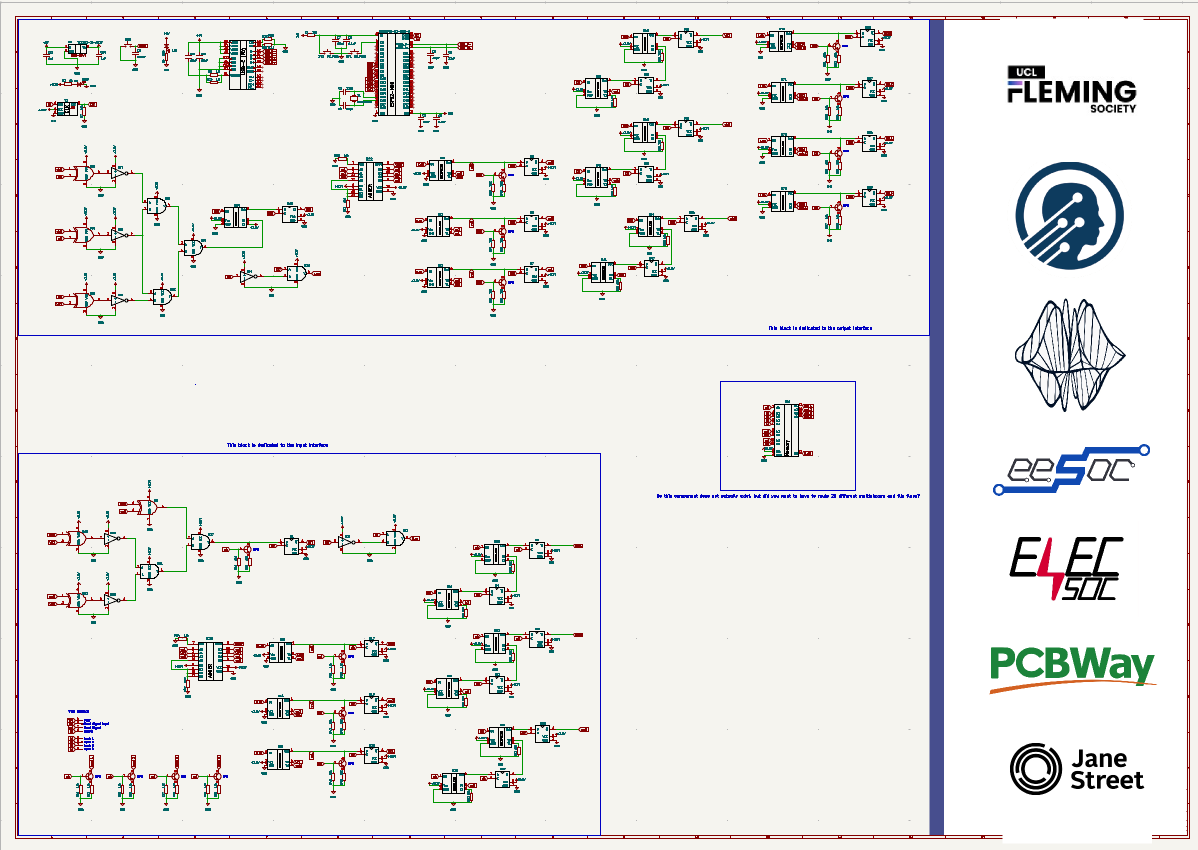
UCL, KCL and Oxford, Cambridge, Imperial and Edinburgh are proud to present the 2026 PCB Challenge. Many thanks to PCBWay and Jane Street for sponsoring the prizes.


If you have any questions please email zceepvb@ucl.ac.uk. Please keep in mind you cannot make a submission/be eligible for the prizes if you do not attend any of the universities organising this event. Within the 7 day period this event is being hosted, any university Engineering society is free to reach out to collaborate at this email address.
All files are meant for KiCAD v10.0, if you have not updated, you probably should. It is a much better version than KiCAD v9.0 (includes dark mode).
The event is running from the 12th of October to the 19th of October.
This challenge invites participants to implement the given schematic as a fully wired PCB in the smallest possible size. As an added challenge the purpose of the PCB itself is left ambiguous. You are provided a schematic with all component values and connections intact, and a footprint associated with each schematic symbol. The event runs fully online, and all the necessary information can be found in this GitHub.
I was inspired to create this challenge by a friend, Taylan Arslan, who gave me what was an essentially impossible challenge to get his PCB to fit within a 40mmx40mm constraint. Despite it being impossible, I learned a lot in those two days trying to accomplish this and the end result is a PCB that I am still very proud of. I hope that participants will also share the same feeling of satisfaction that I got, with the added bonus that this one is not impossible since the smallest possible size is to be determined by one of you.
From my own experience, no matter how much you may like designing PCBs, ultimately it will become a bit repetitive. Thus to make this challenge more interesting; besides the monetary prize; I also decided to make the purpose of the PCB itself a puzzle to be solved.
This challenge will be running for 7 days, until the midnight of October 19th.
Make your submission here: https://forms.cloud.microsoft/Pages/ResponsePage.aspx?id=_oivH5ipW0yTySEKEdmlwtUrHdFLQS5OlbEozvc0DnlUMzJQWkFZVDhVRjZNVTlCQjhHQ0hDSUxSQi4u
Your challenge submission should be a public GitHub repo. In this repo you just need to include the files we need. Your submission for the logic deduction is in the form itself.
The keep out zone of the ESP32 antenna does not have to cover any PCB area, it can be left hanging off the edge of the PCB. Furthermore ignore the datasheets associated with each component in this challenge.
The challenge schematic does include a high speed signal paths (a differential pair requiring a continuous reference plane). It does not however have a significant power delivery requirement (e.g. wide power traces, stitching vias). As such, no specific power plane rules are imposed in this iteration.
1st place: £200
2nd place: £100
3rd place: £50
Top 10: Jane Street Water Bottle
Top 65: Jane Street Tech T-Shirt, 10$ PCBWay Coupon and a PCB Ruler
All participants who submit a valid entry will receive a certificate of participation, a 10$ coupon on orders above 30$ for PCBWay and a PCB ruler from PCBWay. To be classified as a participant you must actually complete the PCB, this meaning that all the connections have been connected with a trace. Auto trace does not count.
Expect the results to be announced within a week or two from the end date of the challenge.
Thank you to our sponsors for making this challenge possible.
| Qty | Value | Footprint | References |
|---|---|---|---|
| 18 | 10k | Capacitor_SMD:C_0603_1608Metric | R7, R10, R11, R12, R13, R14, R16, R17, R18, R19, R21, R22, R23, R25, R26, R27 +2 |
| 16 | 74AUP1G80 | reg:XSON6_SOT1115_NEX | U1, U2, U3, U4, U5, U6, U7, U8, U10, U11, U12, U13, U14, U15, U16, U17 |
| 16 | Q_Dual_NPN_PNP_B1E2B2C2E1C1 | Package_TO_SOT_SMD:SOT-1123 | Q1, Q2, Q3, Q4, Q5, Q6, Q7, Q8, Q9, Q10, Q11, Q12, Q13, Q14, Q15, Q16 |
| 3 | 74LVC1GU04DRL | Package_TO_SOT_SMD:SOT-553 | U19, U20, U24 |
| 2 | 10uF | Capacitor_SMD:C_0603_1608Metric | C15, C20 |
| 2 | 1M | Capacitor_SMD:C_0603_1608Metric | R6, R24 |
| 2 | 1uF | Capacitor_SMD:C_0603_1608Metric | C13, C14 |
| 2 | 5.1k | Resistor_SMD:R_0603_1608Metric_Pad0.98x0.95mm_HandSolder | R15, R20 |
| 2 | CD74HC283M96 | adder:D16 | U22, U23 |
| 1 | 100nF | Capacitor_SMD:C_0402_1005Metric | C9 |
| 1 | 1k | Capacitor_SMD:C_0603_1608Metric | R3 |
| 1 | 330 | Capacitor_SMD:C_0603_1608Metric | R4 |
| 1 | 4068 | AND-8:D14-L | U18 |
| 1 | 74LV1T08GV | Package_TO_SOT_SMD:SC-74A-5_1.55x2.9mm_P0.95mm | U21 |
| 1 | BLED | LED_SMD:LED_0603_1608Metric | D1 |
| 1 | Conn_01x01_Pin | Connector_PinHeader_2.54mm:PinHeader_1x01_P2.54mm_Vertical | J2 |
| 1 | Conn_01x04_Pin | Connector_PinHeader_2.54mm:PinHeader_1x04_P2.54mm_Vertical | J1 |
| 1 | KC2520Z | Oscillator:Oscillator_SMD_Kyocera_KC2520Z-4Pin_2.5x2.0mm | Y2 |
| 1 | LED | LED_SMD:LED_0603_1608Metric | GREEN_LED1 |
| 1 | SW_MEC_5G | Button_Switch_SMD:SW_SPST_CK_RS282G05A3 | SW2 |
| 1 | TC1262-25 | 3v3_ldo:SOT-223_3MC_MCH | U9 |
| 1 | ~ | Connector_USB:USB_C_Receptacle_HCTL_HC-TYPE-C-16P-01A | J3 |
davidlesman/PCB-Challenge-2026
PCB Challenge sponsored by PCBWay and Jane Street

manyetox/PCB-Challenge-4-word-4-bit-asynchronous-FIFO
These were checked with KiCad's DRC and an independent script: - No unconnected items, no clearance, short or crossing errors. - No vias inside any IC courtyard, top or bottom.


Poornimakulkarni26/Carrier-Loader-Unloader
Industrial-grade RP2040 PCB for loader/unloader applications — features 24V tolerant digital inputs for industrial sensors and stepper motor output control for automated pick and place motion.

Terrapin-Rocket-Team/SRAD-Avionics
Code and PCBs for the avionics subteam for the SRAD flight computer and side projects

Shaxzodm2611/4-bit-Adder-Interface-Board
A custom PCB designed to mimic the function of a CPU. Entirely made from discrete logic ICs.


Redherring32/NullCIC
A little board to replace the CIC on the original NES or OpenTendo.
76 parts, built around the 74AUP1G80GF, 74LVC1GU04DRL, CD74HC283M96 and 74LV1T08GVH. The full list of its parts is on this page, with links to each part's symbol and footprint where PCBKit's library has them.
From the MicksTe/PCB-Challenge-2026-Mickey repository on GitHub, at the commit this page was made from: the board is warmup/pcb_challenge.kicad_pcb and its schematic main/pcb_challenge_final.kicad_sch. PCBKit opens the board in the browser, with nothing to install.
Its repository states no licence, so its author keeps all rights: ask MicksTe before reusing the design.