2 layers55.9 × 43.2 mm

 MattisLind/Intellec8
Projects related to the Intellec 8
Intellec8ExtenderBoard is an open-source printed circuit board by MattisLind, from the MattisLind/Intellec8 repository on GitHub. It is a 2-layer board of 203 × 240.2 mm with 57 parts on 95 nets, routed with 614 tracks and 152 vias.
I bought this Intellec 8/80 on a fleamarket outside Stockholm 30 years ago for the equivalent of ten euros. It has been sitting on a shelf since then and now I got the inspiration to fix it. Before doing anything with the machine I dumed the firmware of the EPROMs. 16 1702 EPROM chips. Each of them containing 256 bytes of non-volatile storage. Then I dismantled the entire machine in to pieces and cleaned some 40 years of dust from it. Meanwhile I took quite a lot of photos of the various parts and puth in the Pictures folder.

The first thing to check were the PSU. The Intellec 8 has three PSU assemblies. One provides +5V, another provide +/- 12V and the last one provide -9V and AC for the programming voltage. The -9V supply and the +/- 12V supply worked just fine.
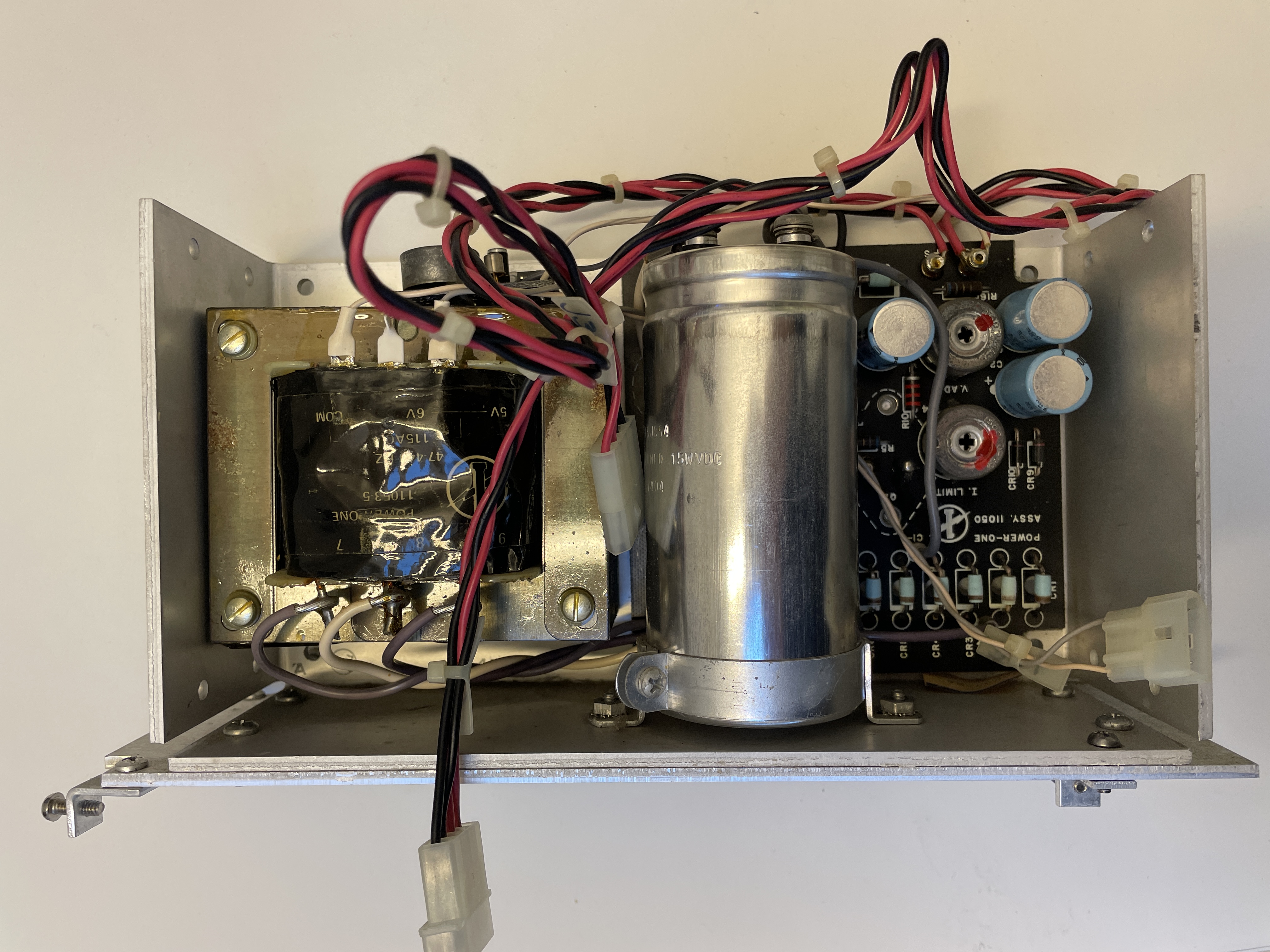
The first thing I tested was the little crowbar addon board. It tripped at almost 9V, a bit to much in my taste, but it was possible to adjust it down to 5.7V. There didn't seemed to be any problems with that other than it was not set correctly.
Then I started working with the PSUs. All off them worked fine except for the +5V PSU that didn't regulate well at all. I had to turn off the crowbare not to make it trip every time. Evverything measured fine, capacitors, carbon composite resistors, forward drop over semiconductor PN-junctions. But it didn't regulate well. Tried to replace the LM723 regulator IC with a NOS IC. But no difference. Then I looked more on the power transistor that acted as a driver for the output stage of the regulator. It was very leaky. With a new power transistor in place the PSU worked fine.
I installed the Front panel controller, CPU and the three memory boards in the backplane and attached the flat cables from the front panel to the front panel controller board and turne the power switch on. There were some kind of activity on the front panel. I could examine and deposit into memory, but RUN mode behaved odd. I wasn't able to single step the CPU but the RUN light could come on. But in RUN mode there were no activity on the FETCH indicator. Strange.
I checked all LEDs on the panel and they seemed to work find as did the switches. To trace problems further I needed to meausure on the front panel controller board. That was quite tricky with the board installed in the backplane. I needed an extender card. So I sat down one Saturday and designed one.

I also inclued test point so it would be easier to attach a logic analyzer if that turned out to be necessary. The more test points the better. And a lot of ground points to be able to attache the ground probes of the LA.
A few weeks later the boards arrived and so did the connector. I choosen a wire-wrap connector which i bent the legs a bit on to make a sturdy connection between the board and the connector.

Now I hade the possibiliy to probe around on the board. The FETCH cycle signal toggled all the time but still the LED was dark. The signal went through a 7417 OC buffer, A3. It turned out that it was always high on the output. A low will cause the LED to be lit. A high will cause it to be turned off. Removed it and tested in my Retro Chip Tester and, yes, it tested bad. A new (date code 1971), tested 7417, was installed and the front panel was a lot happier.
I could enter a short loop at address 0 that was looping back to itself and also single step this little program. Nice!
But when checking the memory at 3800h where the monitor was supposed be located were very strange and did not match the content of the previouslt dumped EPROMs. Pulled out the EPROM board from the backplane and immediatelty saw something that made me suspicous. Two DIP-swicthes. I have had problmes with DIP-switches in the past. And sure enough, closed switches read open-circuit on the meter. Tried to exercise the switches. Tried deoxit, which made it worse. In the end I had to replace them and then with new swicthes in place the memory at 3800h was accessible. I could even start the monitor and saw the LED indicate I/O acces which was likely to be the monitor polling the UART for incoming character.
Now I just have create a current loop adapter and test the I/O card.
3639                          .ORG   3639h
3639   3E FA        RDR:      MVI   A,0FAH
363B   D3 05                  OUT   5
363D   DB 05        RLO:      IN    5
363F   1F                     RAR
3640   1F                     RAR
3641   1F                     RAR
3642   D8                     RC
3643   17                     RAL
3644   DA 3D 36               JC    RLO
3647   DB 04                  IN    4
3649   F5                     PUSH  PSW
364A   3E FB                  MVI   A,0FBH
364C   D3 05                  OUT   5
364E   DB 05        RHI:      IN    5
3650   E6 02                  ANI   02H
3652   CA 4E 36               JZ    RHI
3655   F1                     POP   PSW
3656   2F                     CMA
3657   B7                     ORA   A
3658   C9                     RET
3659                PUNCH:
3659   DB 05                  IN    5
365B E6 10 ANI 010H Jumptable-locatation at 3010 need change to 59H.
| Qty | Value | Footprint | References |
|---|---|---|---|
| 4 | GND | Connector_PinHeader_2.54mm:PinHeader_1x01_P2.54mm_Vertical | J22, J23, J24, J25 |
| 1 | +12V | Connector_PinHeader_2.54mm:PinHeader_1x01_P2.54mm_Vertical | J21 |
| 1 | +5V | Connector_PinHeader_2.54mm:PinHeader_1x01_P2.54mm_Vertical | J12 |
| 1 | -12V | Connector_PinHeader_2.54mm:PinHeader_1x01_P2.54mm_Vertical | J20 |
| 1 | -9V | Connector_PinHeader_2.54mm:PinHeader_1x01_P2.54mm_Vertical | J19 |
| 1 | ADDRESS | Connector_PinHeader_2.54mm:PinHeader_2x08_P2.54mm_Vertical | J3 |
| 1 | CLK PHASE 1 | Connector_PinHeader_2.54mm:PinHeader_1x01_P2.54mm_Vertical | J46 |
| 1 | CLK PHASE 2 | Connector_PinHeader_2.54mm:PinHeader_1x01_P2.54mm_Vertical | J49 |
| 1 | Conn_02x50_Odd_Even | Connector_PCBEdge:INTELLE8_EXT | J2 |
| 1 | Conn_02x50_Odd_Even | Connector_PCBEdge:INTELLE8 | J1 |
| 1 | DATABUS | Connector_PinHeader_2.54mm:PinHeader_2x04_P2.54mm_Vertical | J4 |
| 1 | II BUS | Connector_PinHeader_2.54mm:PinHeader_2x04_P2.54mm_Vertical | J6 |
| 1 | IN BUS | Connector_PinHeader_2.54mm:PinHeader_2x04_P2.54mm_Vertical | J7 |
| 1 | MEMORY DATA | Connector_PinHeader_2.54mm:PinHeader_2x04_P2.54mm_Vertical | J5 |
| 1 | OSC | Connector_PinHeader_2.54mm:PinHeader_1x01_P2.54mm_Vertical | J45 |
| 1 | PROM MOD ENBL | Connector_PinHeader_2.54mm:PinHeader_1x01_P2.54mm_Vertical | J53 |
| 1 | R/~{W} | Connector_PinHeader_2.54mm:PinHeader_1x01_P2.54mm_Vertical | J18 |
| 1 | RAM MOD ENBL | Connector_PinHeader_2.54mm:PinHeader_1x01_P2.54mm_Vertical | J47 |
| 1 | STACK CYCLE | Connector_PinHeader_2.54mm:PinHeader_1x01_P2.54mm_Vertical | J37 |
| 1 | ~{BUS BUSY} | Connector_PinHeader_2.54mm:PinHeader_1x01_P2.54mm_Vertical | J43 |
| 1 | ~{DB OUT} | Connector_PinHeader_2.54mm:PinHeader_1x01_P2.54mm_Vertical | J57 |
| 1 | ~{DBIN} | Connector_PinHeader_2.54mm:PinHeader_1x01_P2.54mm_Vertical | J10 |
| 1 | ~{FETCH CYCLE} | Connector_PinHeader_2.54mm:PinHeader_1x01_P2.54mm_Vertical | J39 |
| 1 | ~{HALT ACK} | Connector_PinHeader_2.54mm:PinHeader_1x01_P2.54mm_Vertical | J56 |
| 1 | ~{HLT INT REQ} | Connector_PinHeader_2.54mm:PinHeader_1x01_P2.54mm_Vertical | J52 |
| 1 | ~{HOLD ACK} | Connector_PinHeader_2.54mm:PinHeader_1x01_P2.54mm_Vertical | J44 |
| 1 | ~{HOLD REQ} | Connector_PinHeader_2.54mm:PinHeader_1x01_P2.54mm_Vertical | J48 |
| 1 | ~{I/O CYCLE} | Connector_PinHeader_2.54mm:PinHeader_1x01_P2.54mm_Vertical | J38 |
| 1 | ~{I/O IN} | Connector_PinHeader_2.54mm:PinHeader_1x01_P2.54mm_Vertical | J11 |
| 1 | ~{I/O OUT} | Connector_PinHeader_2.54mm:PinHeader_1x01_P2.54mm_Vertical | J15 |
| 1 | ~{IN JAM ENBL} | Connector_PinHeader_2.54mm:PinHeader_1x01_P2.54mm_Vertical | J17 |
| 1 | ~{INT CYCLE} | Connector_PinHeader_2.54mm:PinHeader_1x01_P2.54mm_Vertical | J42 |
| 1 | ~{INT DSBL} | Connector_PinHeader_2.54mm:PinHeader_1x01_P2.54mm_Vertical | J50 |
| 1 | ~{INT REQ LTH} | Connector_PinHeader_2.54mm:PinHeader_1x01_P2.54mm_Vertical | J51 |
| 1 | ~{INT REQ} | Connector_PinHeader_2.54mm:PinHeader_1x01_P2.54mm_Vertical | J55 |
| 1 | ~{INTACK} | Connector_PinHeader_2.54mm:PinHeader_1x01_P2.54mm_Vertical | J54 |
| 1 | ~{MEM READ CYCLE} | Connector_PinHeader_2.54mm:PinHeader_1x01_P2.54mm_Vertical | J41 |
| 1 | ~{MEM WRITE CYCLE} | Connector_PinHeader_2.54mm:PinHeader_1x01_P2.54mm_Vertical | J40 |
| 1 | ~{RESET} | Connector_PinHeader_2.54mm:PinHeader_1x01_P2.54mm_Vertical | J14 |
| 1 | ~{SYNCA} | Connector_PinHeader_2.54mm:PinHeader_1x01_P2.54mm_Vertical | J16 |
| 1 | ~{T1} | Connector_PinHeader_2.54mm:PinHeader_1x01_P2.54mm_Vertical | J9 |
| 1 | ~{T2} | Connector_PinHeader_2.54mm:PinHeader_1x01_P2.54mm_Vertical | J31 |
| 1 | ~{T3A} | Connector_PinHeader_2.54mm:PinHeader_1x01_P2.54mm_Vertical | J32 |
| 1 | ~{T3} | Connector_PinHeader_2.54mm:PinHeader_1x01_P2.54mm_Vertical | J26 |
| 1 | ~{T40} | Connector_PinHeader_2.54mm:PinHeader_1x01_P2.54mm_Vertical | J27 |
| 1 | ~{T41} | Connector_PinHeader_2.54mm:PinHeader_1x01_P2.54mm_Vertical | J33 |
| 1 | ~{T42} | Connector_PinHeader_2.54mm:PinHeader_1x01_P2.54mm_Vertical | J28 |
| 1 | ~{T43} | Connector_PinHeader_2.54mm:PinHeader_1x01_P2.54mm_Vertical | J34 |
| 1 | ~{T44} | Connector_PinHeader_2.54mm:PinHeader_1x01_P2.54mm_Vertical | J29 |
| 1 | ~{T45} | Connector_PinHeader_2.54mm:PinHeader_1x01_P2.54mm_Vertical | J35 |
| 1 | ~{T46} | Connector_PinHeader_2.54mm:PinHeader_1x01_P2.54mm_Vertical | J30 |
| 1 | ~{T47} | Connector_PinHeader_2.54mm:PinHeader_1x01_P2.54mm_Vertical | J36 |
| 1 | ~{WAIT ACK} | Connector_PinHeader_2.54mm:PinHeader_1x01_P2.54mm_Vertical | J13 |
| 1 | ~{WAIT REQ} | Connector_PinHeader_2.54mm:PinHeader_1x01_P2.54mm_Vertical | J8 |


tapioki/cephalopoda
Low profile split ergonomic mechanical keyboards

rgoulter/keyboard-labs
Repo with my PCB designs and keyboard firmware

freeDSP/freeDSP-aurora
freeDSP ADAU1452 with 8 analog input, 8 analog outputs, S/P-DIF I/O, ADAT I/O, USB Audio Class2, WiFi, Bluetooth

It measures 203 × 240.2 mm and has 2 copper layers, 1.6 mm thick.
57 parts. The full list of its parts is on this page, with links to each part's symbol and footprint where PCBKit's library has them.
From the MattisLind/Intellec8 repository on GitHub, at the commit this page was made from: the board is ExtenderBoard/Intellec8ExtenderBoard/Intellec8ExtenderBoard.kicad_pcb and its schematic CurrentLoopConverter/CurrentLoopConverter.kicad_sch. PCBKit opens the board in the browser, with nothing to install.
Its repository states no licence, so its author keeps all rights: ask MattisLind before reusing the design.