
2 layers45.5 × 35.5 mm
PWM
AvishkaVishwa/12V-DC-Motor-Speed-Controller-PCB-Design-using-KiCAD
using 555 timer is at Astable mode
16 parts4

A current-limited, inrush-safe low-side load switch for a battery-backed UPS, built entirely from an NE555 timer and a dual op-amp — no dedicated hot-swap/current-limiter IC.
Pcb1 is an open-source printed circuit board by LeoChizh, from the LeoChizh/ups_boards repository on GitHub. It is a 2-layer board of 80 × 125 mm with 27 parts on 15 nets, routed with 160 tracks and 6 vias.
It is built around the LM358, NE555P and IRFZ44N. Its parts include 8 resistors, 6 capacitors, 2 ICs, 2 diodes and 2 crystals.


A current-limited, inrush-safe low-side load switch for a battery-backed UPS, built entirely from an NE555 timer and a dual op-amp — no dedicated hot-swap/current-limiter IC.
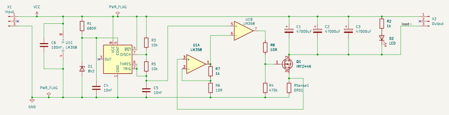
Q1, IRFZ44N).U1A) feeding a PWM comparator (U1B, both halves of one LM358) fold back the MOSFET's duty cycle as current rises, instead of a hard on/off cutoff or a linear-mode limiter (which would dissipate far more heat at these currents).U2), tapped directly off the timing capacitor node rather than OUT.CONT pin (D1, R1) pins the ramp's amplitude to a fixed voltage, so the current limit doesn't drift with input voltage (verified across 12–13.8V).R6 = 10Ω, R7 = 1k (current-sense gain 101×) and RSense1 = 0.01Ω: foldback begins around 4A, full cutoff around 8A — independent of supply voltage.pcb2/pcb1.kicad_sch, pcb2/pcb1.kicad_pcb — the design (KiCad 10)pcb2/myLibrary.pretty/ — custom footprint for the current-sense shunt resistorpcb2/kicad_export_commands.sh — regenerates the ERC/DRC reports, netlist, and laser-burn artwork (copper layer, mirrored/negative variants, and a silkscreen+values placement guide) from the KiCad sourceSingle-sided board. Components are inserted from one face; the copper (opposite face) has its solder mask removed with a laser engraver, then the main power-carrying traces are reinforced with solder for the ~8A current path. See pcb2/pcb1_Fcu_mirrored.svg / pcb2/pcb1_Fcu_mirrored_negative.svg for the burn artwork and pcb2/pcb1_Silkscreen_Values.svg for the component placement guide.
Built and running — powers a Raspberry Pi 4 and WiFi router off a 12V battery bank, verified across repeated input power cycling with no interruption to the load.
This load switch is one module in the larger UPS. The full system schematic shows how it connects to the rest: mains input through breakers into the AC/DC supply and battery charger, a DPDT relay (K1) for mains/battery switchover, over-discharge protection on the battery, and this load switch driving the output USB-C chargers.
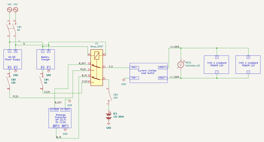
ups_schema/ holds this top-level schematic (KiCad 10, schematic-only — no PCB layout, since it's a system diagram rather than a board to fabricate).
| Enclosure, closed | Enclosure, open |
|---|---|
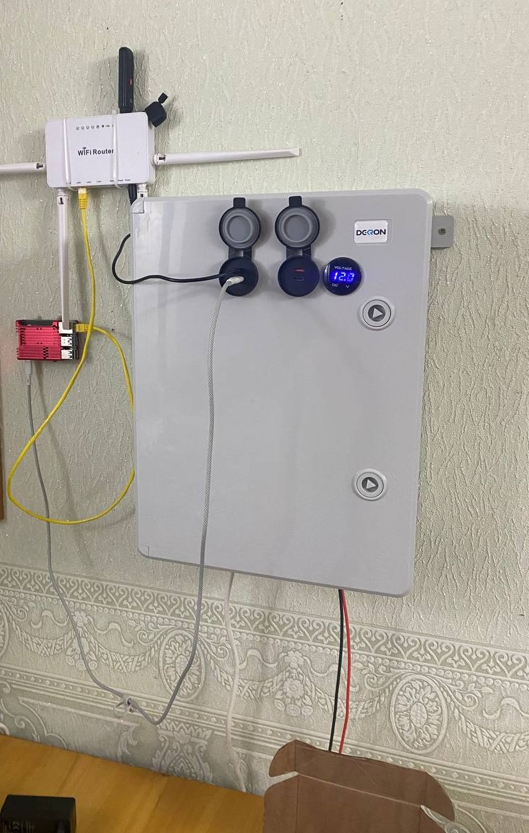 | 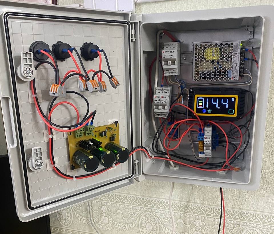 |
This board is mounted on the enclosure door alongside DIN-rail breakers, an AC-DC power supply (230VAC→12VDC), a battery charger, a main relay (230VAC-coil controlled), and an over-discharge protection board. The front panel carries a voltmeter and two 12V-powered USB-C charging ports.
| Qty | Value | Footprint | References |
|---|---|---|---|
| 4 | MountingHole_4.3mm_M4_ISO14580_Pad | MountingHole:MountingHole_4.3mm_M4_ISO14580_Pad | mount, mount, mount, mount |
| 3 | 47000uF | Capacitor_THT:CP_Radial_D35.0mm_P10.00mm_SnapIn | C1, C2, C3 |
| 2 | 10R | Resistor_THT:R_Axial_DIN0207_L6.3mm_D2.5mm_P10.16mm_Horizontal | R6, R8 |
| 2 | 10k | Resistor_THT:R_Axial_DIN0207_L6.3mm_D2.5mm_P10.16mm_Horizontal | R3, R5 |
| 2 | 1k | Resistor_THT:R_Axial_DIN0207_L6.3mm_D2.5mm_P10.16mm_Horizontal | R2, R7 |
| 1 | 0R01 | myLibrary:R_Shunt_d1.2mm_L10mm | RSense1 |
| 1 | 100nf | Capacitor_THT:C_Rect_L9.0mm_W3.3mm_P7.50mm_MKT | C6 |
| 1 | 10nf | Capacitor_THT:C_Rect_L7.0mm_W3.5mm_P5.00mm | C5 |
| 1 | 10nf | Capacitor_THT:C_Rect_L7.2mm_W3.5mm_P5.00mm_FKS2_FKP2_MKS2_MKP2 | C4 |
| 1 | 470k | Resistor_THT:R_Axial_DIN0207_L6.3mm_D2.5mm_P10.16mm_Horizontal | R4 |
| 1 | 680R | Resistor_THT:R_Axial_DIN0207_L6.3mm_D2.5mm_P10.16mm_Horizontal | R1 |
| 1 | 8V2 | Diode_THT:D_DO-35_SOD27_P7.62mm_Horizontal | D1 |
| 1 | IRFZ44N | Package_TO_SOT_THT:TO-220-3_Vertical | Q1 |
| 1 | Input | Connector_Phoenix_MSTB:PhoenixContact_MSTBA_2,5_3-G-5,08_1x03_P5.08mm_Horizontal | X1 |
| 1 | LED | LED_THT:LED_D3.0mm_Clear | D2 |
| 1 | LM358 | Package_DIP:DIP-8_W7.62mm | U1 |
| 1 | NE555P | Package_DIP:DIP-8_W7.62mm | U2 |
| 1 | Output | Connector_Phoenix_MSTB:PhoenixContact_MSTBA_2,5_3-G-5,08_1x03_P5.08mm_Horizontal | X2 |
The 26 most common of 27 parts.
AvishkaVishwa/12V-DC-Motor-Speed-Controller-PCB-Design-using-KiCAD
using 555 timer is at Astable mode

rafliard23/laptopCooler-hardware
Hardware component of my custom laptop cooler project


agusff/Proyecto-Miliohmetro
Proyecto de un milihometro casero para la medicion precisa de resistencias de bajo valor. Trabajo realizado para la catedra de Medidas Electronicas I UTN FRP

BrandonMIsabell/stm32-voltage-regulator-pcb
Routed a custom 5V linear regulator PCB in KiCad to power an STM32 Nucleo board, utilizing an LM358 op-amp and IRFZ44N MOSFET for closed-loop feedback control Fabricated physical hardware from custom Gerber/Drill files…

picli3/dummy-load
Carga electrónica o dummy load basada en LM358 y MOSFET, pensada para probar fuentes de alimentación y convertidores bajo condiciones controladas.

MateoCignetti/ProyectoFinal
Esta obra está bajo una [Licencia Creative Commons Atribución-NoComercial-CompartirIgual 4.0 Internacional][cc-by-nc-sa].

It measures 80 × 125 mm and has 2 copper layers, 1.6 mm thick.
27 parts, built around the LM358, NE555P and IRFZ44N. The full list of its parts is on this page, with links to each part's symbol and footprint where PCBKit's library has them.
From the LeoChizh/ups_boards repository on GitHub, at the commit this page was made from: the board is pcb2/pcb1.kicad_pcb and its schematic pcb2/pcb1.kicad_sch. PCBKit opens the board in the browser, with nothing to install.
Its repository states no licence, so its author keeps all rights: ask LeoChizh before reusing the design.