
2 layers46.8 × 62 mm

 Keyaan-07/fallout-pcb-badge
a shitty badge for the fallout irl hackathon
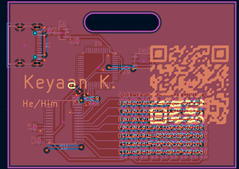
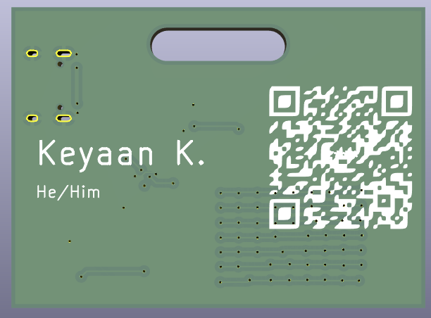
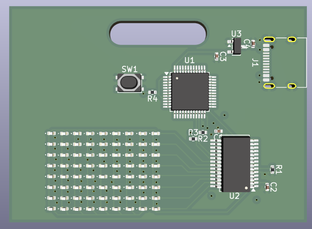
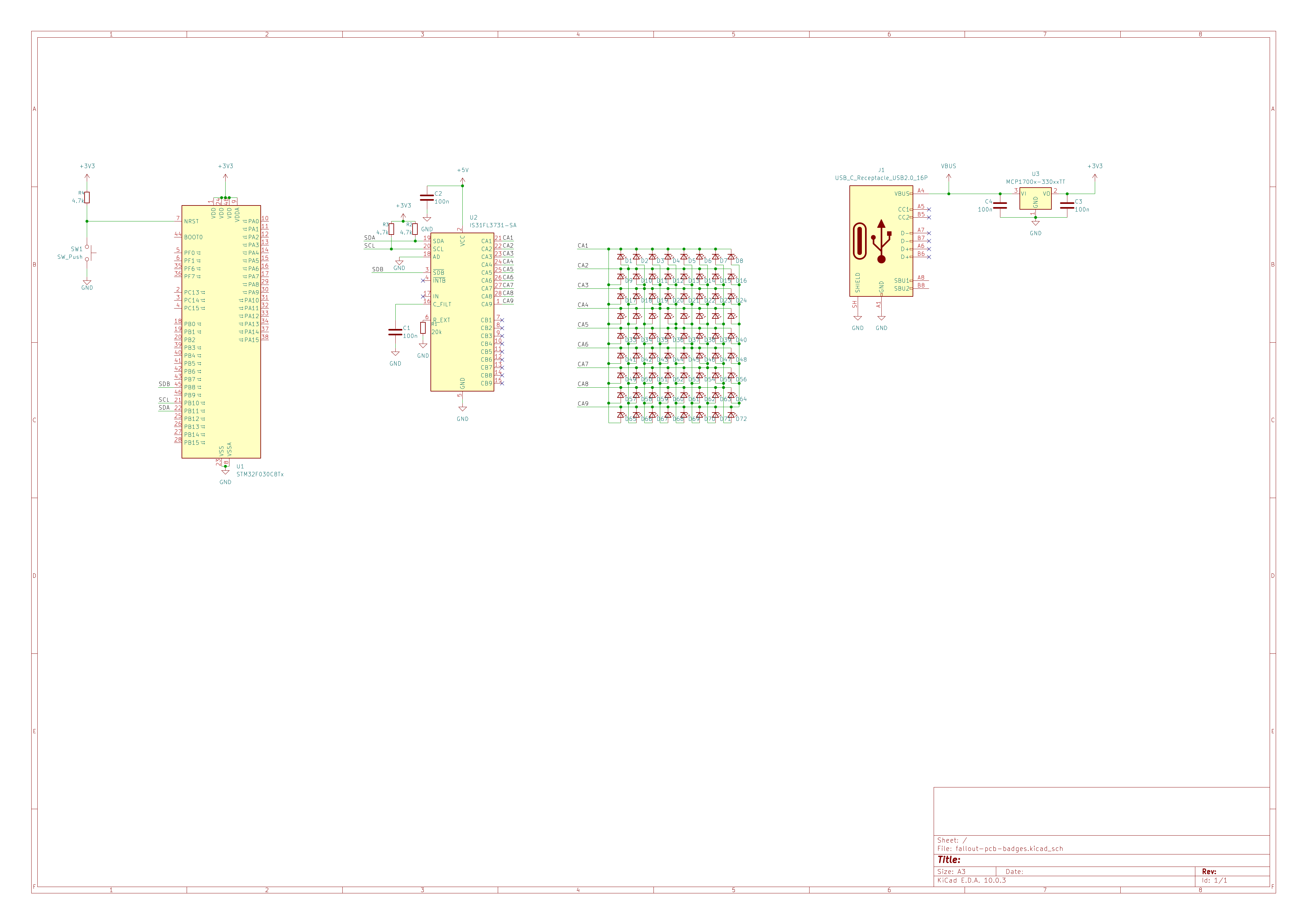
Fallout pcb badges is an open-source printed circuit board by Keyaan-07, from the Keyaan-07/fallout-pcb-badge repository on GitHub. It is a 2-layer board of 55 × 40 mm with 86 parts on 75 nets, routed with 326 tracks and 75 vias.
It is built around the IS31FL3731-SALS2. Its parts include 72 diodes, 4 capacitors, 4 resistors, 3 ICs and 1 connector. It belongs with the lEDs and displays boards and the STM32 boards of this library.
Okay so i made the fallout badge(and everyone else who is a participant made it) andddd i added some unique that that i guess no one might have it. It is decent, it uses an stm32f030.
So the idea i got for the LED matrix was like when i was talking to zach. He was like what are you doing unique in your PCB Badge, so i just formed the idea instantly in my mind and i stuck with it.
Also, while writing this, i got the idea to like add an e-ink, so i am probably gonna add it later, i am really tired rn. I will be buying parts myself. yayay. The bom is js the one that the JLC fab toolkit makes sorry if it's not enough :(
| Qty | Value | Footprint | References |
|---|---|---|---|
| 72 | LED_Small | LED_SMD:LED_0402_1005Metric | D1, D2, D10, D11, D12, D13, D14, D15, D16, D17, D18, D19, D20, D21, D22, D23 +56 |
| 4 | 100n | Capacitor_SMD:C_0402_1005Metric | C1, C2, C3, C4 |
| 3 | 4.7k | Resistor_SMD:R_0402_1005Metric | R2, R3, R4 |
| 1 | 20k | Resistor_SMD:R_0402_1005Metric | R1 |
| 1 | IS31FL3731-SA | Package_SO:SSOP-28_5.3x10.2mm_P0.65mm | U2 |
| 1 | LOGO | LOGO | G*** |
| 1 | MCP1700x-330xxTT | Package_TO_SOT_SMD:SOT-23 | U3 |
| 1 | STM32F030C8Tx | Package_QFP:LQFP-48_7x7mm_P0.5mm | U1 |
| 1 | SW_Push | Button_Switch_SMD:SW_SPST_PTS810 | SW1 |
| 1 | USB_C_Receptacle_USB2.0_16P | Connector_USB:USB_C_Receptacle_XKB_U262-16XN-4BVC11 | J1 |

Tuskar-Marine/hardware
All tools for the Mermaid's Rest open sailing tools


joymonkey/animatrix
open-source hardware, firmware, and software toolkit for custom LED matrix displays

mwuerms/lighthouse_hardware
+ lighthouse + buoy: hand sender, ble advertising


It measures 55 × 40 mm and has 2 copper layers, 1.6 mm thick.
86 parts, built around the IS31FL3731-SALS2. The full list of its parts is on this page, with links to each part's symbol and footprint where PCBKit's library has them.
From the Keyaan-07/fallout-pcb-badge repository on GitHub, at the commit this page was made from: the board is hardware/fallout-pcb-badges.kicad_pcb and its schematic hardware/fallout-pcb-badges.kicad_sch. PCBKit opens the board in the browser, with nothing to install.
Its repository states no licence, so its author keeps all rights: ask Keyaan-07 before reusing the design.