Skip to the content
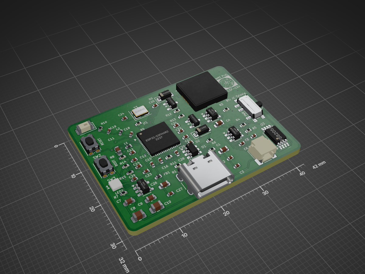
2 layers42 × 32 mmRAMS - PCB, the printed circuit board in 3D

This directory contains the planning, specification, and initial KiCad project for RAMS Wearable PCB Revision C. Do not fabricate from this directory yet -- manual schematic wiring and DRC verification are still needed.

Size
42 × 32 mm
Copper layers
2
Thickness
1.6 mm
Parts
68
Nets
88
Pads
271
Tracks, vias
453, 46
Pours
4
Routed
Yes
KiCad
KiCad 10.0 (file 20260206)
Created
5 Sep 2026
Updated
7 Nov 2026

Overview

RAMS - PCB is an open-source printed circuit board by JanClyde05, from the JanClyde05/Road-Accident-Monitoring-System repository on GitHub. It is a 2-layer board of 42 × 32 mm with 68 parts on 88 nets, routed with 453 tracks and 46 vias.

It is built around the ESP32-S3FH4R2, AP2112K-3.3 and DW01A, with the 1N4148W, 2450AT18D0100E and AO3401A among its other parts. Its parts include 29 capacitors, 15 resistors, 5 ICs, 4 diodes and 3 transistors. It belongs with the ESP32 boards of this library.

Main components

12

README

hardware/KiCAD Files/Antigravity Build/RAMS - PCB - Rev C/README.md

RAMS Rev C -- engineering work in progress

This directory contains the planning, specification, and initial KiCad project for RAMS Wearable PCB Revision C. Do not fabricate from this directory yet -- manual schematic wiring and DRC verification are still needed.

Status: Phase 2 complete (KiCad project generated)

Completed

  • Phase 1: Circuit Definition
    • Identified all 5 critical defects from Rev A
    • DOST-ASTI EPDC manufacturing constraints extracted
    • 68 components cataloged with verified datasheet pinouts
    • FS8205A SOT-23-6 pinout verified (S1=1, D1=2, S2=3, G2=4, D2=5, G1=6)
    • DW01A, LTH7R, 2450AT18B100E pinouts verified
    • WROOM-1 module internal VDDA confirmed (no external connection needed)
    • Firmware GPIO cross-check passed (12/12 GPIOs match config.h)
    • Self-check script: zero errors
  • Phase 2: KiCad Project Creation
    • Project file with EPDC design rules (0.30mm track, 0.254mm space, 0.40mm drill)
    • Structural schematic generated (68 components in 10 functional blocks)
    • PCB board generated (42x32mm, rounded corners, ground zones, antenna keepout)
    • Custom antenna footprint for 2450AT18B100E (3216 2-terminal)
    • Ground stitching via grid on both layers
    • Net classes: Default, Power (0.50mm), RF_50R, USB

Next: Phase 3 (Manual KiCad work)

  • Open schematic in KiCad, resolve library symbols
  • Wire component pins according to circuit_spec.json net assignments
  • Run ERC, fix errors
  • Import netlist to PCB
  • Place footprints in functional zones
  • Route critical paths (power, USB, RF) manually
  • Route remaining signals with interactive router
  • Run DRC, verify EPDC compliance
  • Generate Gerber + drill files for EPDC

User decisions recorded

  • WS2812B: 5050 SMD (standard package)
  • Board size: Minimize, targeting 42x32mm
  • USB-C: TYPE-C-31-M-12, shell slots converted to 1.0mm round holes for EPDC
  • Solder mask: Black board, white silkscreen
  • EPDC castellation: Open -- user needs to confirm with EPDC

Key corrections from Rev A

  • Q3: SOT-23-6 correct pinout (was TSSOP-8 with wrong wiring)
  • ANT1: 2450AT18B100E = 2-terminal feed+NC (correct 3216 footprint)
  • LED1: GPIO48 (was GPIO46)
  • MCU: WROOM-1 module (was bare QFN-56 incompatible with EPDC)
  • All design rules comply with DOST-ASTI EPDC limits
  • Ground continuity enforced with stitching via grid

Files

FilePurpose
00_REVISION_PLAN.mdComplete revision plan with defects, constraints, verification gates
DECISIONS.mdUser-confirmed design decisions
circuit_spec.jsonComponent definitions, pin mappings, net assignments (68 components)
EPDC_DESIGN_RULES.mdKiCad design rules for DOST-ASTI EPDC compliance
RESEARCH_LEDGER.mdDatasheet source references
ERROR_LOG.mdDocumented Rev A mistakes with corrective actions
RAMS - PCB.kicad_proKiCad project with EPDC rules and net classes
RAMS - PCB.kicad_schStructural schematic (needs manual wiring in KiCad)
RAMS - PCB.kicad_pcbPCB board outline, zones, keepouts, stitching vias
RAMS_Local.pretty/Custom footprint library (2450AT18B100E antenna)
build_schematic.pySchematic generator from circuit_spec.json
build_board.pyPCB board generator
verify_circuit_spec.pyAutomated circuit spec self-check

Parts

68
QtyValueFootprintReferences
110.1uFCapacitor_SMD:C_0402_1005MetricC2, C5, C6, C13, C14, C15, C16, C20, C27, C28, C29
510uFCapacitor_SMD:C_0603_1608MetricC1, C7, C9, C11, C26
51uFCapacitor_SMD:C_0402_1005MetricC3, C12, C17, C22, C23
3100kResistor_SMD:R_0402_1005MetricR6, R7, R13
212pFCapacitor_SMD:C_0402_1005MetricC24, C25
21kResistor_SMD:R_0402_1005MetricR5, R12
247uFCapacitor_SMD:C_0805_2012MetricC8, C10
25.1kResistor_SMD:R_0402_1005MetricR1, R2
2KMR2Button_Switch_SMD:SW_Push_1P1T_NO_CK_KMR2SW2, SW3
10RResistor_SMD:R_0402_1005MetricR10
110kResistor_SMD:R_0402_1005MetricR8
110nFCapacitor_SMD:C_0402_1005MetricC21
1180kResistor_SMD:R_0402_1005MetricR15
11N4148WDiode_SMD:D_SOD-123D3
12.4nHInductor_SMD:L_0402_1005MetricL2
12.4pFCapacitor_SMD:C_0402_1005MetricC19
12.7pFCapacitor_SMD:C_0402_1005MetricC18
122RResistor_SMD:R_0402_1005MetricR9
12450AT18D0100ERF_Antenna:Johanson_2450AT18x100ANT1
12nHInductor_SMD:L_0402_1005MetricL1
1330RResistor_SMD:R_0402_1005MetricR4
1330kResistor_SMD:R_0402_1005MetricR14
133RResistor_SMD:R_0402_1005MetricR11
14.02kResistor_SMD:R_0402_1005MetricR3
14.7uFCapacitor_SMD:C_0603_1608MetricC4
140MHzCrystal:Crystal_SMD_3225-4Pin_3.2x2.5mmY1
1AO3401APackage_TO_SOT_SMD:SOT-23Q1
1AP2112K-3.3Package_TO_SOT_SMD:SOT-23-5U5
1Ai-Thinker-Ra-02RF_Module:Ai-Thinker-Ra-01-LoRaU2
1BC817-25Package_TO_SOT_SMD:SOT-23Q2
1DW01APackage_TO_SOT_SMD:SOT-23-6U4
1ESP32-S3FH4R2Package_DFN_QFN:QFN-56-1EP_7x7mm_P0.4mm_EP4x4mmU1
1FS8205APackage_SO:TSSOP-8_4.4x3mm_P0.65mmQ3
1FerriteBeadInductor_SMD:L_0402_1005MetricFB1
1LOGOLOGOG***
1LTH7RPackage_TO_SOT_SMD:SOT-23-5U3
1MSK12C02Button_Switch_SMD:SW_SPDT_PCM12SW1
1SK6805-EC20rams:LED_SK6805_EC20_2.0x2.0mmLED1
1SM02B-SRSS-TBConnector_JST:JST_SH_SM02B-SRSS-TB_1x02-1MP_P1.00mm_HorizontalJ2
1SMD-9650-3327rams:Buzzer_SMD_9650_3327BZ1
1SS14WDiode_SMD:D_SOD-123D2
1TYPE-C-31-M-12USB_C_TYPE_C_31_M_12J1
1USBLC6-2SC6Package_TO_SOT_SMD:SOT-23-6D1

More from JanClyde05/Road-Accident-Monitoring-System

2
  • 2 layers48 × 38 mmRAMS RevC, the printed circuit board in 3D

    RAMS RevC

    JanClyde05/Road-Accident-Monitoring-System

    This directory contains the planning, specification, and initial KiCad project for RAMS Wearable PCB Revision C. Do not fabricate from this directory yet -- manual schematic wiring and DRC verification are still needed.

    68 parts1
  • 2 layers42 × 32 mmRAMS - PCB, the printed circuit board in 3D

    RAMS - PCB

    JanClyde05/Road-Accident-Monitoring-System

    This directory contains the planning, specification, and initial KiCad project for RAMS Wearable PCB Revision C. Do not fabricate from this directory yet -- manual schematic wiring and DRC verification are still needed.

    67 parts1

Similar boards

  • 4 layers45 × 32.5 mmFlashKa panel, the printed circuit board in 3D

    FlashKa panel

    DomPka/LuxLibre

    Pick a light · Compare · Web apps · Firmware · Design your own · Build a FlashKa · Repository map · Help

    143 partsGPL-3.0
  • 4 layers30.3 × 90.5 mmTinker base, the printed circuit board in 3D

    Tinker base

    Tinkerbug-Robotics/TinkerRocket

    Model rocket flight computer, ground station, iOS app, and simulation

    94 parts1GPL-3.0
  • 2 layers35 × 100 mmWalkieTalkie, the printed circuit board in 3D

    WalkieTalkie

    GuzziFlipFlops/ESP32-Walkie-Talkie

    An open source ESPNOW based walkie talkie with a 600 meter tested distance, with an OLED and multiple buttons to interact with

    66 parts7MIT
  • 2 layers96 × 50 mmPager, the printed circuit board in 3D

    Pager

    justinlindh/bramble

    Privacy-first LoRa mesh networking for ESP32-S3, built with ESP-IDF

    97 parts2MIT
  • 2 layers45 × 100 mmWalkiepcb, the printed circuit board in 3D

    Walkiepcb

    houseofthe051010/ESP32-Walkie-Talkie-V2

    This ESP32 Walkie Talkie is redesigned with a SX1262 radio, a PCB, and a full case redesign.

    93 parts1
  • 4 layers62 × 46.9 mm4LayerLabProject, the printed circuit board in 3D

    4LayerLabProject

    ZharbolatDinmukhamed/Haptic-Glove-PCB

    A wrist-mounted PCB for a haptic feedback glove, developed as part of my Research Assistantship at the Tactile Laboratory, Nazarbayev University.

    122 parts
  • 2 layers214 × 174 mmSoundBoxSTM32 cheap, the printed circuit board in 3D

    SoundBoxSTM32 cheap

    DominikNeugebauer/PCB

    All of my pcb projects i have made so far

    134 parts
  • 2 layers34 × 132 mmSugarboat, the printed circuit board in 3D

    Sugarboat

    kitspace-test-repos/kicad6-file-collection

    51 partsMIT

Questions

How big is the RAMS - PCB PCB?

It measures 42 × 32 mm and has 2 copper layers, 1.6 mm thick.

What parts does the RAMS - PCB use?

68 parts, built around the ESP32-S3FH4R2, AP2112K-3.3, DW01A and 1N4148W. The full list of its parts is on this page, with links to each part's symbol and footprint where PCBKit's library has them.

Where can I download the RAMS - PCB KiCad files?

From the JanClyde05/Road-Accident-Monitoring-System repository on GitHub, at the commit this page was made from: the board is hardware/KiCAD Files/Antigravity Build/RAMS - PCB/RAMS - PCB.kicad_pcb and its schematic hardware/KiCAD Files/Antigravity Build/RAMS - PCB - Rev B/RAMS - PCB.kicad_sch. PCBKit opens the board in the browser, with nothing to install.

Can I use the RAMS - PCB design in my own project?

Its repository states no licence, so its author keeps all rights: ask JanClyde05 before reusing the design.