This platform is designed with the intention of providing an interactive educational opertunity to university students with diverse technical backgrounds on switching regulators (namely buck converters).
Load 5R is an open-source printed circuit board by Infineon, from the Infineon/voltage-regulator-learning-platform repository on GitHub. It is a 2-layer board of 100 × 100 mm with 141 parts on 33 nets, routed with 29 tracks and 2,915 vias.
Its parts include 135 resistors and 1 connector.
README
README.md
Learning Platform for Switching Regulators
This platform is designed with the intention of providing an interactive educational opertunity to university students with diverse technical backgrounds on switching regulators (namely buck converters). The project aims to develop the students' skills on using basic microcontroller IO features as starters and then build upon those skills to use a gate driver to implement a buck converter and monitor its output and efficiency. Along the Buck converter design process, the students get to use the the on board's peripherals to understand the different properties of buck converters and how they could be optimized.
Project's History
The project was introduced as a bachelor thesis of Lukas Wiegert. (version 1.0). Continued and further developed by Adrian Keil (Versions: 1.0 ,1.1 ,1.2) and finalized by Youssef Tarkhan (versions: 2.0, 2.1). The latest update was done 2025 from David Lopez (version: PCBv3). The boards are used by the Technical University of Munich to teach the students and assess the quality and functionality of these boards and provide an open source curriculum.
Latest Update PCBv3
The latest update included mainly following changes:
Removing the 3.3V rail. Only two remaining power supply rails (12V for power part, 5V for digital logik and measurements).
Fixed common error that current measurement opamps burn because of shorted ouputs (male pinheaders get easily shorted when probed)
Additional output resistance as second safety measure
Board Breakdown
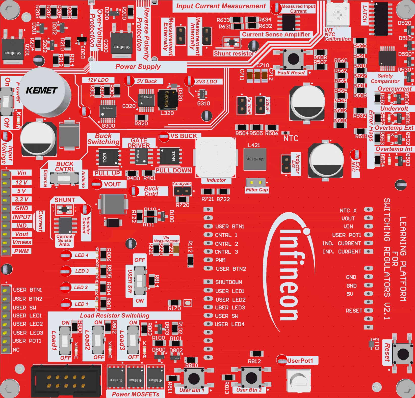
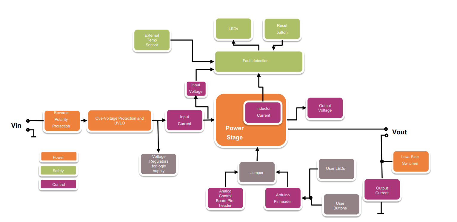
Brief summary: As you can see from the block diagram, the board needs an input connection. (Bannana ports are provided at the bottom side of the board). After the board makes sure that the polarity and the voltage are in check, the power is fed into the board's internal powersupply compartment. If the voltage level is below 10V then you will observe the undervoltage LED glowing in RED. The powerline feeding the whole board interfaces two optional possibilities for input current measurement. Power is then fed onto the power stage which consists of the components needed for the buck switching with a VOut output (In older versions of the board there used to be additional banana ports for the Vout terminal and an additional ground banana port.) Power is additionally fed into the arduino peripherals for basic microcontroller usage (LEDS, Switches, Buttons and Potentiometers).
Note that for every measurable quantity such as the input current for instance, there is a testpoint that could be attached onto an oscilloscope in order to have an easier experience when trying the measure this quantity
Microcontroller Pinouts
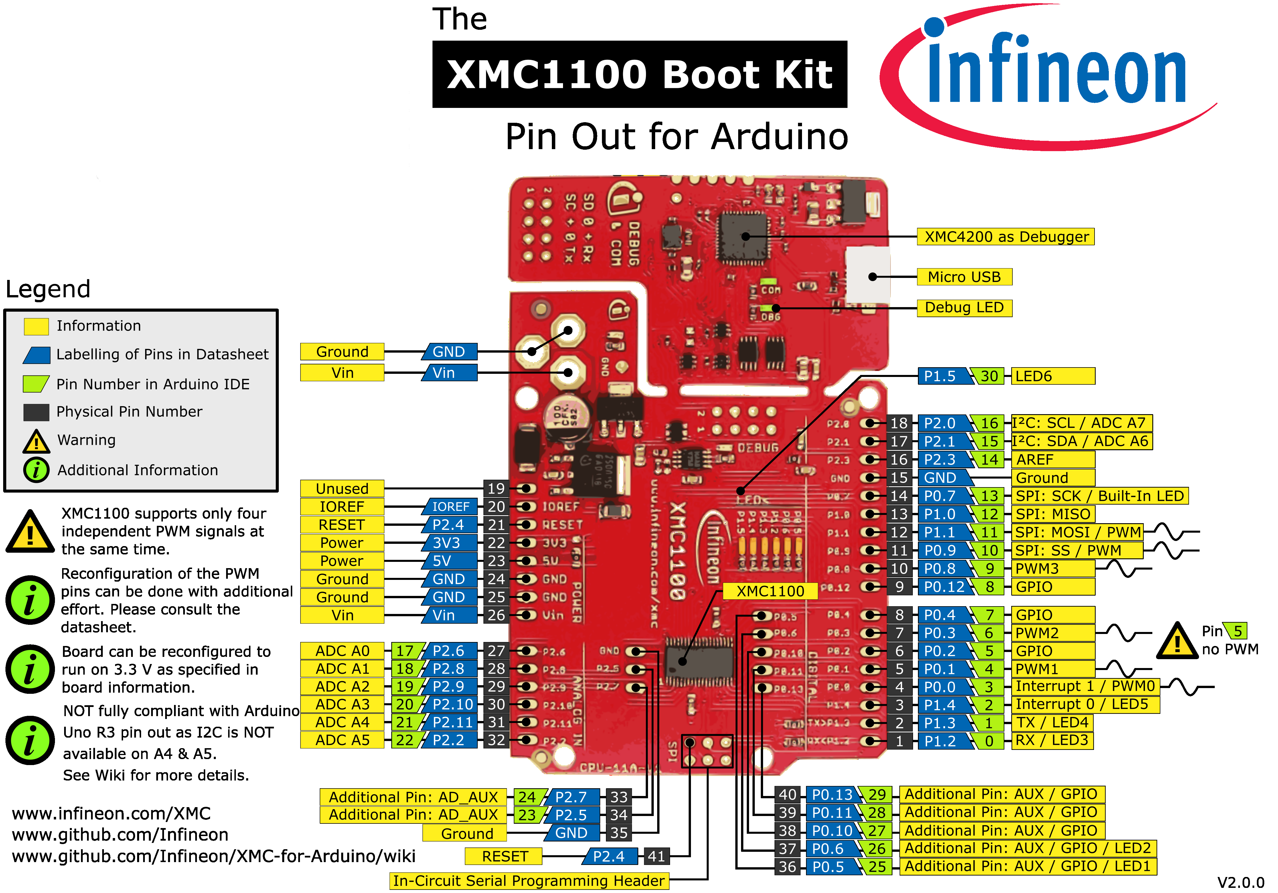
This platform is an arduino compatable shield. It is intended to be used in combination with the XMC1100 Bootkit
The labelling of the XMC1100 Bootkit pins is placed on the bottom layer's silk screen.
An Arduino compatible shield is a hardware expansion board that is designed to be compatible with Arduino microcontroller boards. It is called a "shield" because it typically attaches on top of an Arduino board, extending its capabilities and providing additional functionalities
XMC 1100 Bootkit Pins
Pin
Net
Type
Description
A0
In_Curr_ADC
Input
Analog input for current measurement
A1
Inductor_Current_ADC
Input
Analog input for inductor current sensing
A2
UserPot1
Input
Analog input for user potentiometer 1
A3
Vin_Meas
Input
Analog input for voltage measurement
A4
Vout_Meas
Input
Analog input for output voltage measurement
A5
NTC_ext
Input
Analog input for external NTC temperature
D0
NC
NC
Not connected
D1
NC
NC
Not connected
D2
UserBtn1
Input
Digital input for user button 1
D3
Cntrl1
Output
Digital output for control signal 1
D4
Cntrl2
Output
Digital output for control signal 2
D5
Cntrl3
Output
Digital output for control signal 3
D6
Buck_Cntrl_Arduino
Output
Digital output for Arduino buck control
D7
UserBtn2
Input
Digital input for user button 2
D8
Shutdown
Input
Digital input for shutdown signal
D9
User_LED1
Output
Digital output for user LED 1
D10
User_LED2
Output
Digital output for user LED 2
D11
User_LED3
Output
Digital output for user LED 3
D12
UserSw
Input
Digital input for user switch
D13
User_LED4
Output
Digital output for user LED 4
Note: The following code snippet defines all the required arduino pins for using the platform, simply copy it to the beginning of your code (before the setup)
cpp
// Define all Arduino pins// Digital Out
#define USER_LED1 9
#define USER_LED2 10
#define USER_LED3 11
#define USER_LED4 13
#define BUCK_PIN 6// Digital In
#define USER_BTN1 2
#define USER_BTN2 7
#define SHUTDOWN 8
#define USER_SW 12// Analog In
#define IN_CURR A0
#define INDUCTOR_CURR A1
#define USER_POTI A2
#define VIN_MEAS A3
#define VOUT_MEAS A4
#define NTC A5
Also add the following pin setup lines into your setup loop
cpp
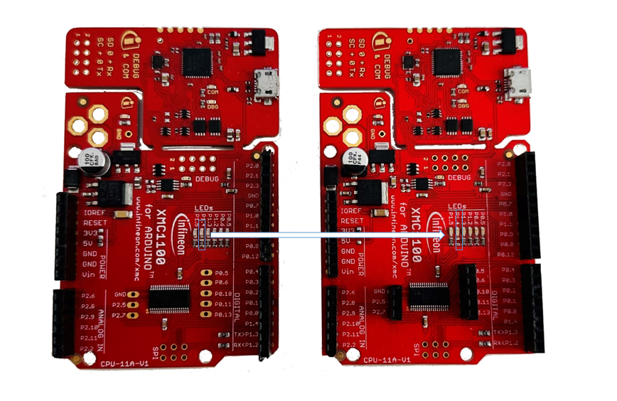
Note: In order to use both user buttons you'll have to unsolder the resistor at Pin 1.4 (check out the diagram below)
Power Input
The board is equipped with a variety of safety measures to ensure that it not only has a long life, but also ensure that students get to have a higher level of freedom with it. The board is to be powered with a DC power supply through banana plugs.
First stage of the power input is going through the reverse polarity protection circuit, following by over voltage detection circuit. ( In case of an overvoltage detection, power is cut from the main circuit through a MOSFET) Note that the board supports up to 30V but has a recommended to be used in the 15V input range
Voltage is then delivered to the board compartments : Powersupply, Safety Comparator, Powerstage stage & Miscellaneous
Power Supply
The Optimum input Voltage for the board input is around 15V. In case the voltage goes over 19V the board goes into a hysterisis where it only gets back in operation when the voltage level goes below ****. Feel free to check the simulation files if you want to get a deeper insight into how the hysterisis works on a circuit design level. (You will have to install the spice model files for the ATL431, click here for a guide on how to do that)
Along with the input being fed into the board, the board additionally has 3 additional power components which are:
12V LDO:
- Gate driver IC
- Input Internal Current Sense Amplifier
- Safety Latch
- Safety Circuit Comparator
- Safety LEDs
- Output Internal Current Sense Amplifier
- ADC Compensation for MCU Input
- Safety Comparator Circuit
Safety
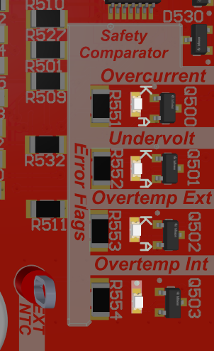
The safety compartment of the board is comprised mainly of a comparator and a safety latch, where when the safety comparator detects a flag, this flag is saved on the latch. (To reset the latch all you'll have to do is press the latch reset button)
For example if the undervoltage flag is raised (Input voltage goes below 10V), the undervoltage flag will be raised and the corresponding LED will turn on. Aslong as the latch has not been reset, even if the input voltage goes above 10V, the LED will stay on and the shutdown signal will keep getting sent to the microcontroller and the power components.
Flags
When safety flags are triggered, a shutdown signal is generated and the corresponding flag's LED is lit. The shutdown signal is delivered to the microcontroller and the power stage components. The powerstage is disabled as long as the shutdown signal is being delivered to its components.
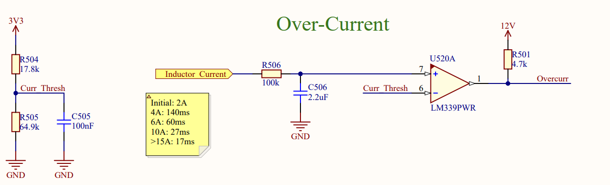
Overcurrent
The output current from the powerstage is measured over a shuntresistor and a current sense amplifier. The output signal is then fed into a the safety comparator, which is compared to a constant reference voltage. (This reference voltage is equal to the corresponding output of the amplifier when the output current is around 2.8A).
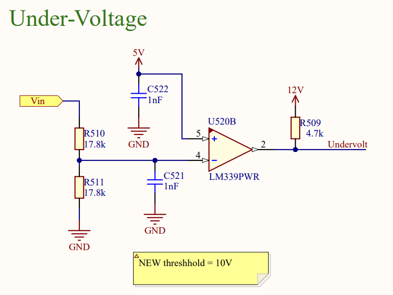
Undervoltage
the input voltage is fed through the two equal value resistors R510 and R511 and the signal is halfed (voltage divider Law), and is then fed into the comparator. As reference the 5V Buck output is fed into the other input of the comparator. If the input voltage goes below 10V , then half of that signal will be lower than 5V and so the undervoltage flag would be triggered.
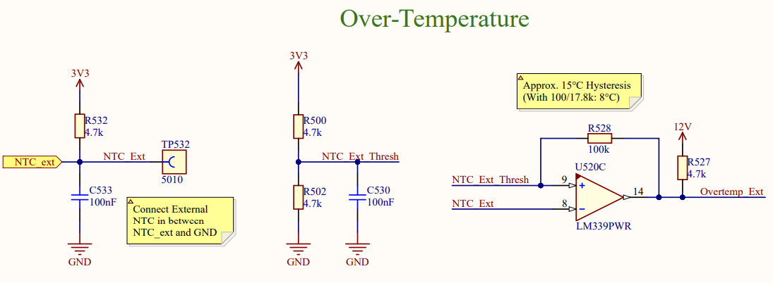
Overtemperature (External)
An NTC is connected on the external resistor board. (Negative Thermal cooefficient resistor; pretty much a fancy word for a resistor, who's resistance value changes when its temperature changes). The NTC's signal is connected to an input of the safety comparator with a reference signal connected to the other input.
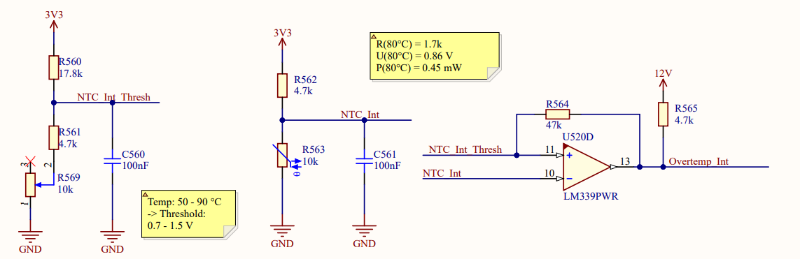
Overtemperature (Internal)
Similar to external overtemperature detection, however the NTC is onboard and there is a variable resisotr on board to calibrate the onboard overtemperature limit of the board.
Safety Flag LEDs
you can find the safety LEDs are placed on the top right corner of the PCB
Miscellaneous
The board is equipped with:
1 User programmable potentiometer
2 User programmable buttons
4 User programmable LEDs
1 User programmable Switch
Buck Operation
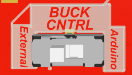
The buck operation takes place over a gate driver; what happens: is that the gate driver takes in pulse width modulated signals from the microcontroller (XMC 1100 Bootkit) or an external controller through the PWM pin on the external control pin header. The users have to modify the BUCK CNTRL switch to adapt the circuitry to whether or not the control signal would be coming from the external control pin header or through the onboard controller pins. The students get to change the frequency and duty cycle of the signal in order to achieve their desired output voltage.
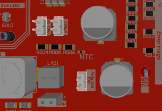
There are also some jumpers on board that could adjust the output circuity of the buck operation.
Jumpers are available for:
Connecting three 10 uF Capacitors
Connecting a 220uF capacitor
Connecting a 15uH inductor
External Control
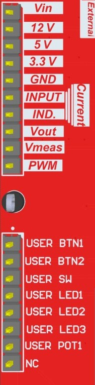
Aside from using the board as a shield, it could also just be connected to an external controller circuit.
As shown in the diagram above, using jumper cables, the user externally has access to:
Input voltage to through the Banana cables
12V Output of the LDO
5V Output of the Buck Controller
3.3V Output of the LDO
Input Current Sensor Reading
Output Current Sensor Reading
Output Voltage
Output Voltage (Calibrated to 0 to 5V)
External Buck Control
User Button 1 Input
User Button 2 Input
User Switch Input
User LEDs (1 to 3)
User Potentiometer 1 Input
NTC Calibration
For making sure that the temperature on board is in check, negative thermal coefficient resistors are chosen . The onboard maximum temperature could easily be calibrated by adjusting a potentiometer for temperature limitation between (50°C and 90°C)
Current Measurement
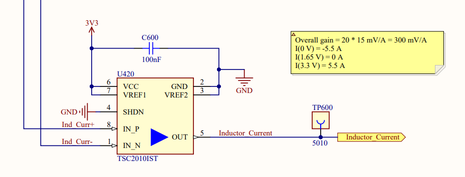
The main method of current measurement is the combination of a shunt resistor and a current sense amplifier. This setup is repeated in the input and output current measurement system. The operation relies on a voltage drop accross the shunt resistor proportional to the current flowing through it. This voltage drop is amplified by the current sense amplifier into a new voltage value. This voltage value is read by the micro-controller's ADC and it's used to subsequently calculate the value of the current.
the main component (TSC2010IST) in the diagram above is a current sense amplifier. This current sense amplifier is connected over a shunt resistor (pins: 1 & 8). The output of this amplifier is proportional to the amount of current going through the shunt resistor.
Testpoints
The board is equiped with test points to make it easier for students to observe different quantities using an oscilloscope.
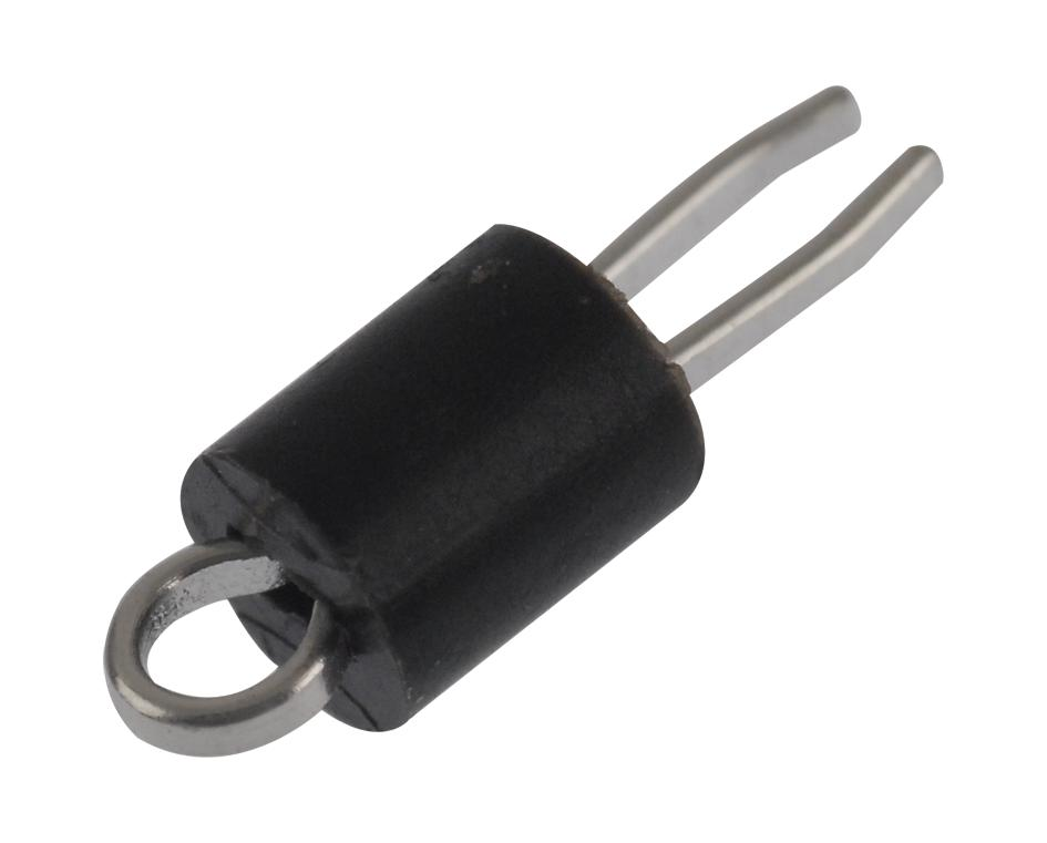
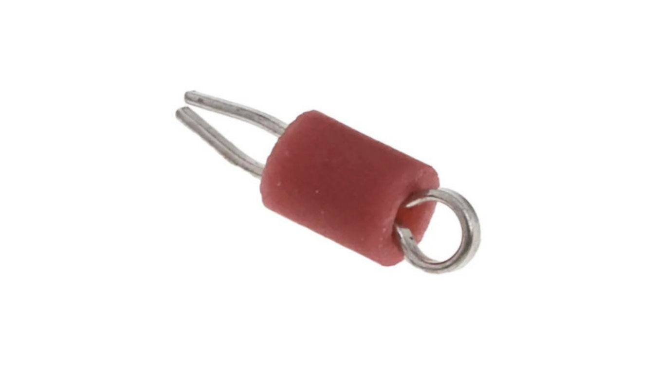
All black testpoints are Ground testpoints
Red testpoints are labelled with their corresponding measurement quantity.
Simulation Files
To provide a rich experience to students, the simulation files for most of the building blocks of the learning platform are provided. These simulations are accessable on LTSPICE, which is an open source freeware, that is very popular in the industry.
You can find these simulations under the Directory /Simulations.
Future Strategy
This project is not yet fully disclosed, and it will remain under development so feel free to reach out to youssef.tarkhan@infineon.com for any inquiries or suggestions anytime.
This platform is designed with the intention of providing an interactive educational opertunity to university students with diverse technical backgrounds on switching regulators (namely buck converters).
Open source Real-Time Quantitative PCR Implementation
141 parts48GPL-3.0
Questions
How big is the Load 5R PCB?
It measures 100 × 100 mm and has 2 copper layers, 1.6 mm thick.
What parts does the Load 5R use?
141 parts. The full list of its parts is on this page, with links to each part's symbol and footprint where PCBKit's library has them.
Where can I download the Load 5R KiCad files?
From the Infineon/voltage-regulator-learning-platform repository on GitHub, at the commit this page was made from: the board is Load Resistors/Discrete Resistors/Load_5R/Load_5R.kicad_pcb. PCBKit opens the board in the browser, with nothing to install.
Can I use the Load 5R design in my own project?
Its repository states no licence, so its author keeps all rights: ask Infineon before reusing the design.