
4 layers25 × 35 mm
Qfn csi underpad diff
drandyhaas/KiCadRoutingTools
A set of Python/Rust tools to aid routing in KiCad
2 parts744MIT

 HorstBaerbel/GBA-mem21
Game Boy Advance faster EWRAM hack
GBA mem is an open-source printed circuit board by HorstBaerbel, from the HorstBaerbel/GBA-mem repository on GitHub, published under the MIT licence. It is a 4-layer board of 18.2 × 18.3 mm with 2 parts on 47 nets, routed with 321 tracks and 44 vias.
It is built around the IS62WV12816EBLL-45TLI. It belongs with the retro computing and games boards of this library.
Here be dragons🐉!
This killed my GBA. I probably fried the power supply IC. I'm leaving this here for academic purposes...
The GBA has 256kB of external work RAM in the form of an 128kx16 SRAM chip with 70ns (M68AS128DL70N6), 85ns (μPD442012AGY-BB85X-MJH), or even 120ns (HY62LF16206A-LT12C) access time, depending on the chip (good hardware database here). The regular EWRAM access speed is 2 wait states (3/3/6 clock cycles) for 1/2/4 bytes of data. Setting the undocumented EWRAM wait states flags to 0Eh allows you to speed up EWRAM access to 1 wait state (2/2/4 clock cycles). Setting it to 0Fh will crash / lock up the GBA though, because 0 wait states are out of the specs of all SRAM chips ever used in the GBA / GBA SP and GBA Micro (access times must be < 62ns) and EWRAM gets corrupted (see testing memory). The choice of those SRAM chips back in 2000 was probably due availability and keeping the system costs down, but 20 years later there are cheap SRAM chips available with as low as 10ns access time, so...
This aims to replace the GBAs SRAM chip with a faster chip on a carrier board, because there seem to be no pin-compatible models anymore. The old models used a TSOP-I-48 footprint, newer models use a TSOP-II-44 footprint and all have a very different pinout.
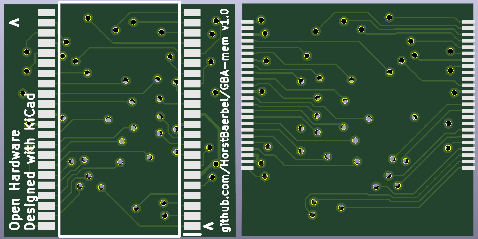
All pins have been connected straight through, with the exception of /CS1 (/CE1) and CS2 (CE2) which are permanently connected to GND resp. VDD2 / 2.5V anyway according to GBATEK. Also the upper byte lines (D8-D15) are swapped for better chip placement.
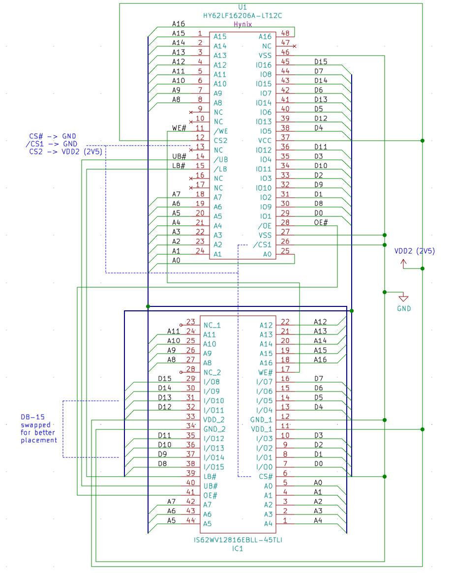
Supposedly compatible SRAM chips for the board:
| Model | min. access time | max. power draw | working |
|---|---|---|---|
| IS62WV12816BLL-55TLI / -55BLI | 55ns | ~25mA | NO (tested) |
| IS62WV12816EBLL-45TLI | 45ns | ~15mA | ? |
| CY62136FV30LL-45ZSXIT / -45ZSXI / -45ZSXA | 45ns | ~18mA | ? |
| CY62136ESL-45ZSXI | 45ns | ~20mA | ? |
The power draw of the replacement chips seems to be comparable to that of the originals. I'd go with the IS62WV12816EBLL-45TLI if you can find it, because of the lowest power draw.
The KiCad directory contains the schematics and PCB layout and also gerber files (exported for JLPCB). I chose JLPCB as a manufacturer in this case and a board thickness of 0.8mm. Remember to get a stencil made for both sides.
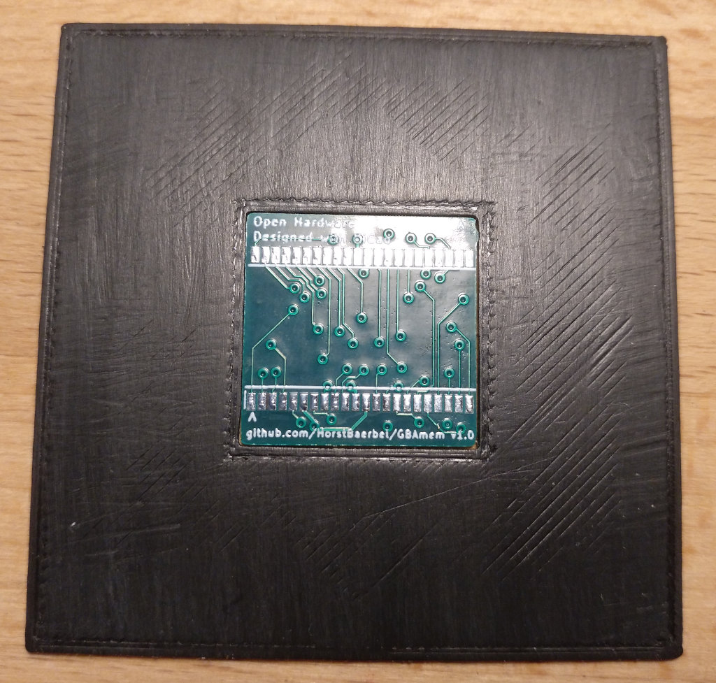
I opted for ChipQuik Sn42/Bi58 TS391LT solder paste because of its low melting point of 138°C. This makes it easier to solder and you need to heat up the GBA mainboard less. You can 3D-print a PCB holder for the PCB to apply solder paste with the stencil:
You can use the MemTestGBA binary to test stability and performance (on a REAL AGB/AGS Game Boy Advance, NOT on the DS / DS lite or a GBA micro):
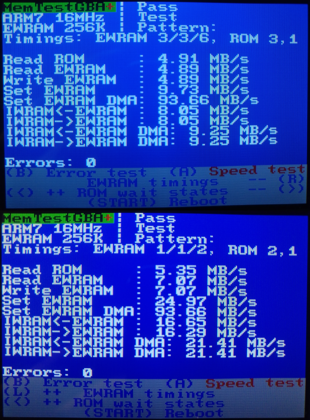
It will test the ROM read, EWRAM read / write and IWRAM ⟷ EWRAM copy speed (startup default, Button A). Memory is copied in 24kB blocks, so this is not the max. speed possible, but gives a ballpark number. You can also test the memory for errors (Memtest86+-like, Button B). Buttons L and R let you increase or decrease the EWRAM timings, ⟵ and ⟶ let you increase or decrease the ROM wait states and START reboots the GBA. The source code can be found in the src directory.
Theoretical EWRAM SRAM chip transfer speeds should be: Clock speed * 2 (16 bit SRAM width) / (1 + wait states) ⟷ 16 * 1024 * 1024 * 2 / (1 + w) = 10.6 MB/s (default 2 wait states) and 32 MB/s (0 wait states).
mkdir build && cd build
cmake -DCMAKE_BUILD_TYPE=Release ..
make -j $(grep -c '^processor' /proc/cpuinfo 2>/dev/null)If you want to build your own soft- or hardware based on this, you can. See the MIT LICENSE.
The "Modern DOS" 8x8 font is from Jayvee Enaguas and used by CC0.
The CMake build scripts / toolchain is from Thomas Farr and uses the MIT LICENSE.
| Qty | Value | Footprint | References |
|---|---|---|---|
| 1 | HY62LF16206A-LT12C | HY62LF16206A-LT12C:HY62LF16206A-LT12C_TSOP-I-48_12x18mm_Flip | U1 |
| 1 | IS62WV12816EBLL-45TLI | IS62WV12816EBLL-45TLI:SOP80P1176X120-44N | IC1 |
drandyhaas/KiCadRoutingTools
A set of Python/Rust tools to aid routing in KiCad


dbalsom/arduinoX86
An interface between an Arduino Due or Arduino GIGA and 8088, 8086, V20, V30, 186 or 286 CPUs

agranlund/raven
Homemade MC68060 + DSP56303 Atari-compatible computer. Hardware, firmware, and software stack


imendizabal/Near-Field-Probes
Open Source kit of Near Field Probes for Electromagnetic Compatibility (EMC) troubleshooting
It measures 18.2 × 18.3 mm and has 4 copper layers, 1.6 mm thick.
2 parts, built around the IS62WV12816EBLL-45TLI. The full list of its parts is on this page, with links to each part's symbol and footprint where PCBKit's library has them.
From the HorstBaerbel/GBA-mem repository on GitHub, at the commit this page was made from: the board is KiCad/GBAmem.kicad_pcb. PCBKit opens the board in the browser, with nothing to install.
Its repository publishes it under the MIT licence: you may reuse it on that licence's terms (keep the author's notice, and for a copyleft licence share your changes alike).