4 layers114.3 × 13 mm
H Field 18mm
imendizabal/Near-Field-Probes
Open Source kit of Near Field Probes for Electromagnetic Compatibility (EMC) troubleshooting
2 parts59GPL-3.0

 imendizabal/Near-Field-Probes59
Open Source kit of Near Field Probes for Electromagnetic Compatibility (EMC) troubleshooting
E Field 10cm is an open-source printed circuit board by imendizabal, from the imendizabal/Near-Field-Probes repository on GitHub, published under the GPL-3.0 licence. It is a 4-layer board of 99.7 × 13 mm with 2 parts on 2 nets, routed with 15 tracks and 192 vias.
It belongs with the sensors and measurement boards of this library.
This repository provides KiCAD PCB designs and documentation for Near-Field Probes used in EMC troubleshooting
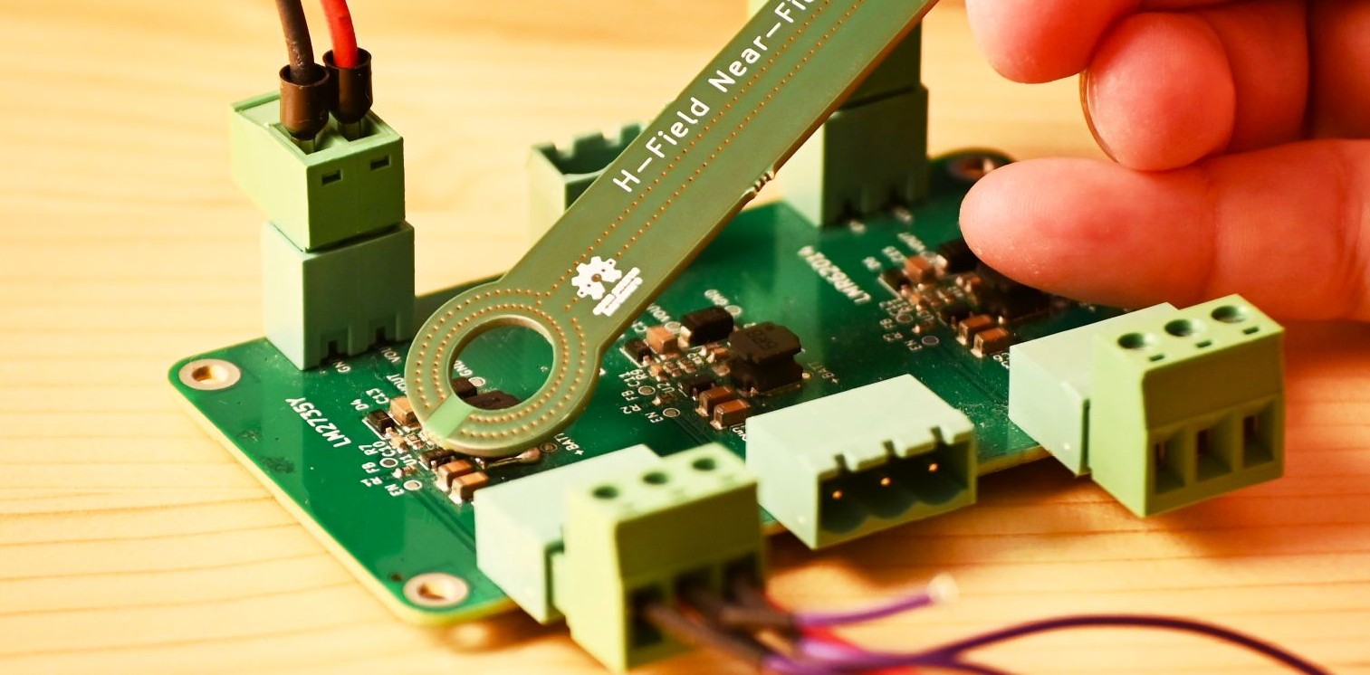
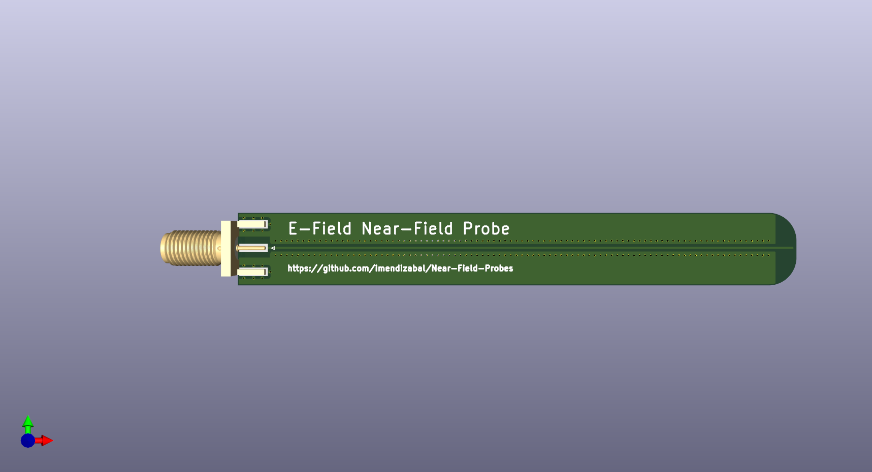
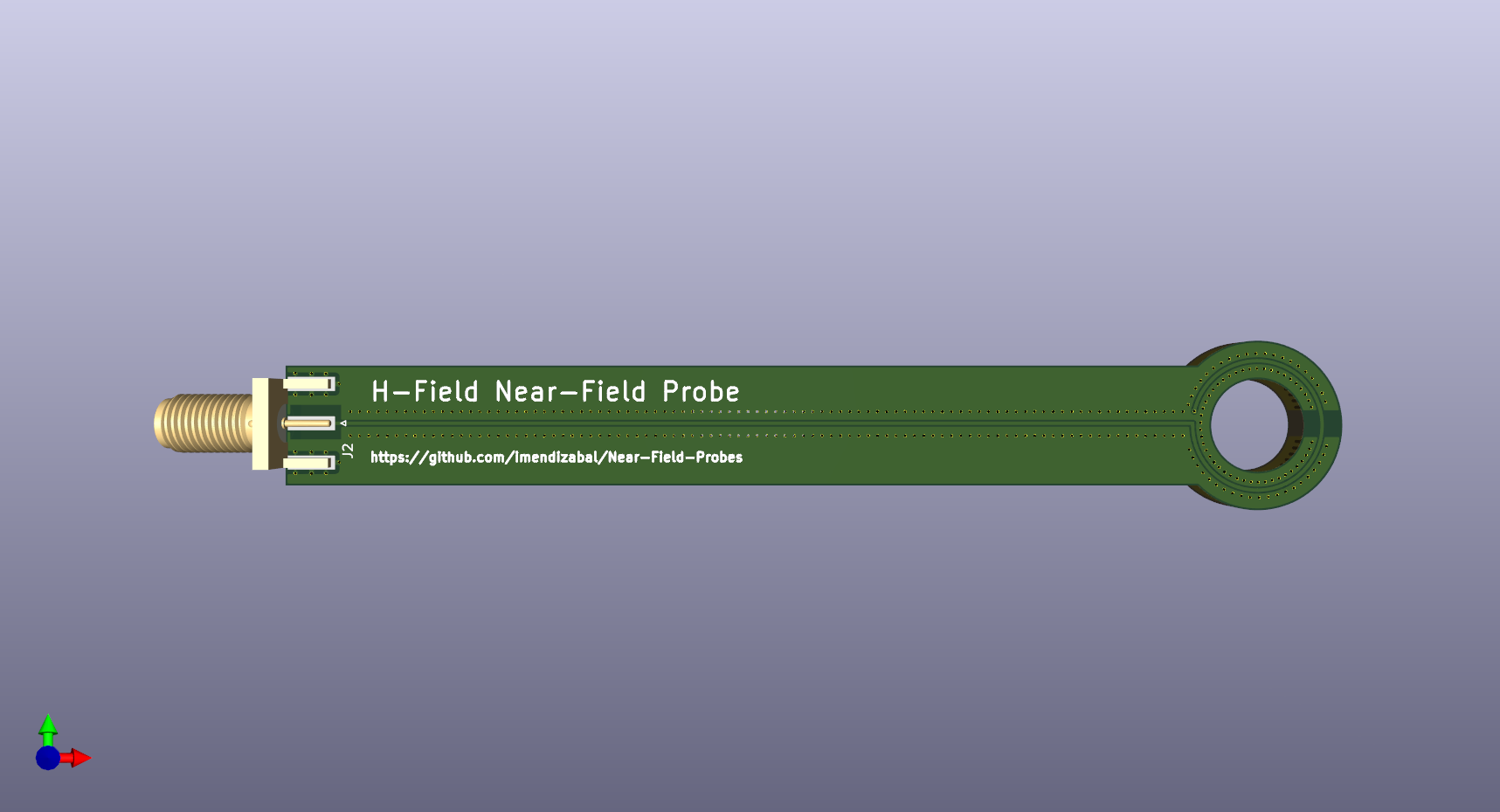
Contributions are welcome! Feel free to submit pull requests with improvements or new probe designs.
This project is licensed under the GNU General Public License (GPL) – you are free to use, modify, and distribute it, but any derivative work must also be open-source under the same license.
Interference Technology Page - What You Need to Know to Design Your Own Kit of Near-Field Probes
Ey, I am Ignacio! 👋🏼
I’m an electronic designer and EMC fan with experience helping companies across automotive, industrial, medical, and IoT sectors solve EMC challenges at the design stage. My goal is to make EMC accessible, affordable and understandable. I love creating content and making complex concepts easy.
This work exists because of the contribution of other amazing designers and creatives
| Qty | Value | Footprint | References |
|---|---|---|---|
| 1 | Conn_Coaxial_Small | Connector_Coaxial:SMA_Amphenol_132289_EdgeMount | J1 |
The 1 most common of 2 parts.
imendizabal/Near-Field-Probes
Open Source kit of Near Field Probes for Electromagnetic Compatibility (EMC) troubleshooting

drandyhaas/KiCadRoutingTools
A set of Python/Rust tools to aid routing in KiCad


dbalsom/arduinoX86
An interface between an Arduino Due or Arduino GIGA and 8088, 8086, V20, V30, 186 or 286 CPUs

agranlund/raven
Homemade MC68060 + DSP56303 Atari-compatible computer. Hardware, firmware, and software stack


It measures 99.7 × 13 mm and has 4 copper layers, 1.59 mm thick.
2 parts. The full list of its parts is on this page, with links to each part's symbol and footprint where PCBKit's library has them.
From the imendizabal/Near-Field-Probes repository on GitHub, at the commit this page was made from: the board is E-Field 10cm/E-Field 10cm.kicad_pcb and its schematic E-Field 10cm/E-Field 10cm.kicad_sch. PCBKit opens the board in the browser, with nothing to install.
Its repository publishes it under the GPL-3.0 licence: you may reuse it on that licence's terms (keep the author's notice, and for a copyleft licence share your changes alike).