2 layers248.3 × 147.3 mm
PCB BOARD DESIGN FOR IOT ENABLED WEARABLE HEALTH MONITOR
NITHYAR2005/PCB-BOARD-DESIGN-FOR-IOT-ENABLED-WEARABLE-HEALTH-MONITOR
9 parts

 Habib-creater/MAX30102_Optical_Sensor_Board
MAX30102-based optical sensor board designed for embedded hardware development.
Max30102 pcb is an open-source printed circuit board by Habib-creater, from the Habib-creater/MAX30102_Optical_Sensor_Board repository on GitHub. It is a 2-layer board of 26.3 × 18 mm with 18 parts on 15 nets, routed with 111 tracks and 29 vias.
It is built around the MAX30102, AP2112K-3.3 and SMAJ5.0A. Its parts include 6 capacitors, 3 resistors, 3 ICs, 1 diode and 1 connector. It belongs with the sensors and measurement boards of this library.


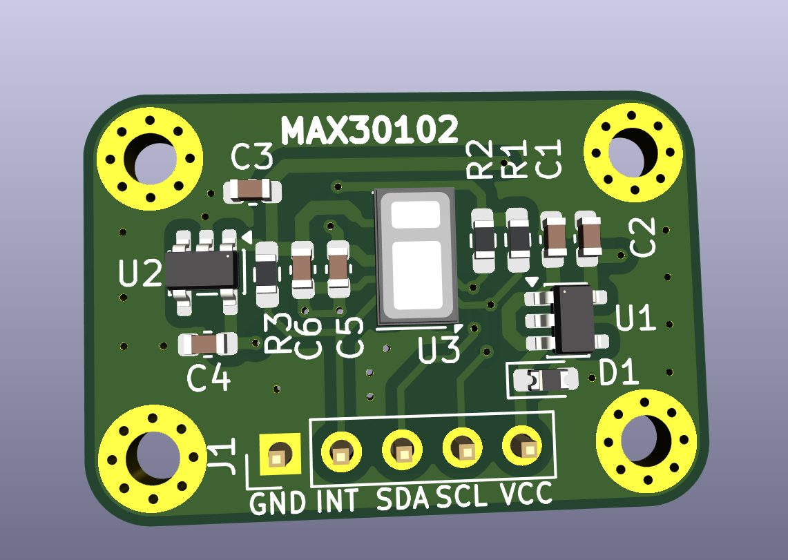
MAX30102 • Dual Supply Rails • I²C • 2-Layer PCB • KiCad
A compact optical sensing board centered on the MAX30102 integrated pulse-oximetry and heart-rate sensor.
Schematic • BOM • Gerbers • KiCad Files
The MAX30102 Optical Sensor Board is a compact 2-layer PCB designed around the MAX30102 sensor.
The board provides the MAX30102 with dedicated supply regulation, I²C connectivity, interrupt access, and a 5-pin external interface.
The complete hardware design package is included in this repository, covering the native KiCad project, schematic, PCB layout, BOM, Gerber and drill manufacturing files, pick-and-place data, and board documentation.
| Resource | Description |
|---|---|
| Schematic PDF | Electrical schematic |
| Bill of Materials | Component BOM |
| Gerber & Drill Files | PCB manufacturing data |
| KiCad Project | Native KiCad design files |
| Board Images | 3D renders and PCB views |
| Pick-and-Place Data | Component placement files |
| Feature | Details |
|---|---|
| Optical Sensor | MAX30102 |
| Sensor Function | Pulse oximetry and heart-rate sensing |
| Digital Interface | I²C |
| Interrupt | Dedicated INT connection |
| Input Supply | +5 V |
| Logic / Sensor Rail | +3.3 V |
| LED Supply Rail | +1.8 V |
| 3.3 V Regulator | AP2112K-3.3 |
| 1.8 V Regulator | TLV70018 |
| Protection | SMAJ5.0A TVS diode |
| External Interface | 1×5 pin header |
| PCB | 2-layer |
| EDA Software | KiCad |
| PCB Thickness | 1.6 mm |
| Manufacturing Data | Gerber + PTH/NPTH drill |
| Assembly Data | Pick-and-place CSV |
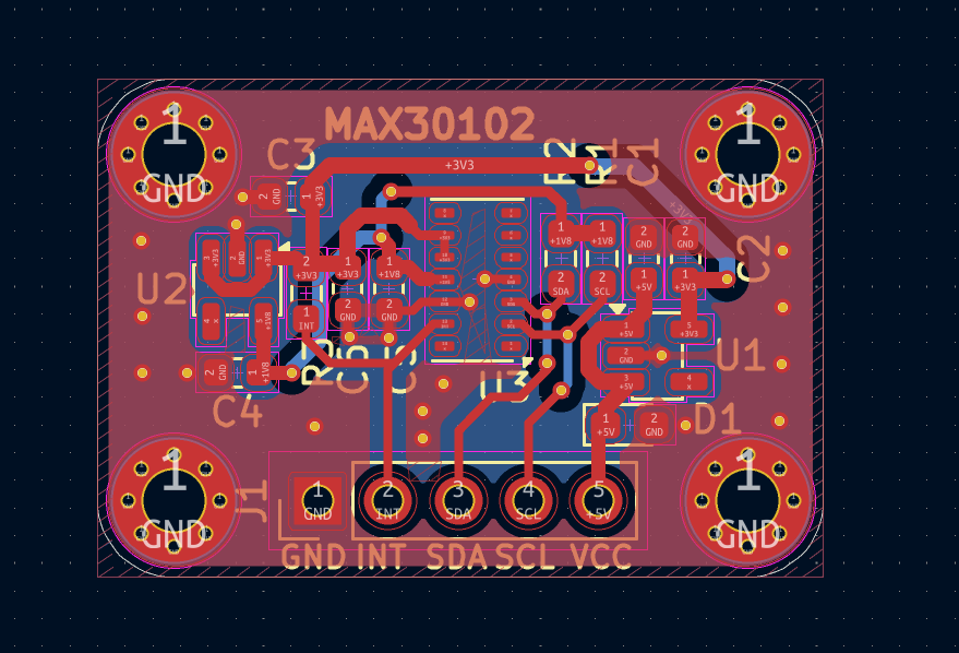
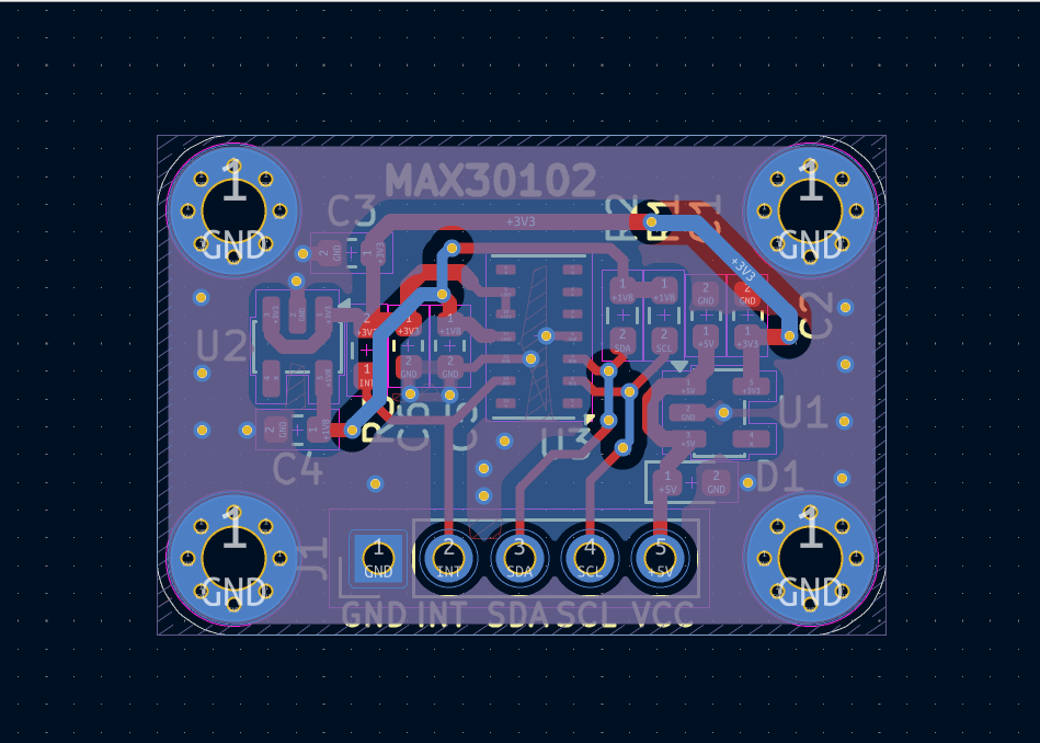
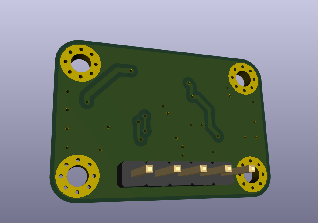
The board is organized around the MAX30102 sensor and its associated power and interface circuitry.
The MAX30102 integrates optical sensing functionality for pulse-oximetry and heart-rate applications.
The sensor interface exposes:
The board contains dedicated regulation stages for the sensor system:
A 5-pin header provides the primary external connection to the board.
| Pin | Signal |
|---|---|
| 1 | +3.3 V |
| 2 | GND |
| 3 | +5 V |
| 4 | SCL |
| 5 | SDA |
The interrupt signal is routed to the MAX30102 interface circuitry.
The board is implemented as a 2-layer PCB using KiCad.
The native KiCad project is located in:
| File | Description |
|---|---|
max30102_pcb.kicad_pro | KiCad project |
max30102_pcb.kicad_sch | Schematic source |
max30102_pcb.kicad_pcb | PCB layout |
The exported schematic PDF is available in docs/.
The manufacturing package is available in:
The package contains:
The component BOM is available in:
The BOM contains the component references, quantities, values, footprints, and available manufacturer/supplier information associated with the design.
Assembly placement data is available in:
The package contains separate top-side and bottom-side component position CSV files.
The repository includes:
| Item | Status |
|---|---|
| Schematic | ✅ Completed |
| PCB Layout | ✅ Completed |
| PCB Layer Count | ✅ 2-layer |
| KiCad Project | ✅ Included |
| BOM | ✅ Included |
| Gerber Files | ✅ Generated |
| Drill Files | ✅ Generated |
| Pick-and-Place Data | ✅ Included |
| Documentation | ✅ Included |
.
├── hardware/
│   └── kicad/
│       ├── max30102_pcb.kicad_pro
│       ├── max30102_pcb.kicad_sch
│       └── max30102_pcb.kicad_pcb
│
├── manufacturing/
│   ├── gerbers/
│   │   ├── max30102_pcb-F_Cu.gbr
│   │   ├── max30102_pcb-B_Cu.gbr
│   │   ├── max30102_pcb-F_Silkscreen.gbr
│   │   ├── max30102_pcb-B_Silkscreen.gbr
│   │   ├── max30102_pcb-F_Mask.gbr
│   │   ├── max30102_pcb-B_Mask.gbr
│   │   ├── max30102_pcb-F_Paste.gbr
│   │   ├── max30102_pcb-B_Paste.gbr
│   │   ├── max30102_pcb-Edge_Cuts.gbr
│   │   ├── max30102_pcb-PTH.drl
│   │   ├── max30102_pcb-NPTH.drl
│   │   └── max30102_pcb-job.gbrjob
│   │
│   └── pick-and-place/
│ ├── max30102_pcb-top-pos.csvThe hardware design files in this repository are licensed under the CERN Open Hardware Licence Version 2 - Strongly Reciprocal (CERN-OHL-S-2.0).
The licence permits use, modification, distribution, and manufacture under the terms of the CERN-OHL-S-2.0 licence, with the corresponding source-sharing requirements for covered hardware.
Copyright © 2026 Habib Ur Rehman
See LICENSE for the licence identifier and official
licence reference.
Electronics Engineering
Embedded systems, PCB design, microcontrollers, electronics hardware, and hardware development.
MAX30102 Optical Sensor Board
Compact Open Hardware Sensor Platform
| Qty | Value | Footprint | References |
|---|---|---|---|
| 4 | MountingHole_Pad | MountingHole:MountingHole_2.2mm_M2_Pad_Via | H1, H2, H3, H4 |
| 3 | 4.7K | Resistor_SMD:R_0603_1608Metric_Pad0.98x0.95mm_HandSolder | R1, R2, R3 |
| 2 | 0.1u | Capacitor_SMD:C_0603_1608Metric | C5, C6 |
| 2 | 10u | Capacitor_SMD:C_0603_1608Metric | C1, C2 |
| 1 | 1u | Capacitor_SMD:C_0603_1608Metric | C3 |
| 1 | 2.2u | Capacitor_SMD:C_0603_1608Metric | C4 |
| 1 | AP2112K-3.3 | Package_TO_SOT_SMD:SOT-23-5 | U1 |
| 1 | Conn_01x05_Pin | Connector_PinHeader_2.54mm:PinHeader_1x05_P2.54mm_Vertical | J1 |
| 1 | MAX30102 | OptoDevice:Maxim_OLGA-14_3.3x5.6mm_P0.8mm | U3 |
| 1 | SMAJ5.0A | Diode_SMD:D_0603_1608Metric_Pad1.05x0.95mm_HandSolder | D1 |
| 1 | TLV70018_SOT23-5 | Package_TO_SOT_SMD:SOT-23-5 | U2 |
NITHYAR2005/PCB-BOARD-DESIGN-FOR-IOT-ENABLED-WEARABLE-HEALTH-MONITOR

Protocentral/protocentral_pulse_express_hardware
Open-source hardware design files for the ProtoCentral Pulse Express MAX30102 + MAX32664D breakout

RobuGabrie/skydiver
Real-time skydiver monitoring for instructors and jump teams. The system combines a BLE wearable, an offline-first Expo mobile app, Supabase persistence, and a responsive Next.js dashboard with safety analytics.

sutyazz/Resume-Projects
A comprehensive collection of engineering and computer science projects demonstrating expertise across multiple domains including embedded systems, web development, machine learning, signal processing, and hardware…

KIIT-Robotic-Society/Dharma_RoboFest4.0
Dharma Bot is a quadruped robotic dog featuring 12-DOF locomotion, real-time sensing, and a modular subsystem design.

byui-formula-hybrid/legacy-Cooling-Pump-Board
BYUI Cooling pump CAN control board

desvandi/PLTSMonitoring_Firmware-Backend
Integrated to PLTSMonitoring_PWA

fsanzeni/FSC-BT1104QI-Breakout
Breakout board for Feasycom FSC-BT1104QI (Bluetooth 5.4 / QCC3095) with USB-C/UART bridge, 3.3V LDO regulation, I2S digital audio, differential speaker outputs, and all pads broken out.
It measures 26.3 × 18 mm and has 2 copper layers, 1.6 mm thick.
18 parts, built around the MAX30102, AP2112K-3.3 and SMAJ5.0A. The full list of its parts is on this page, with links to each part's symbol and footprint where PCBKit's library has them.
From the Habib-creater/MAX30102_Optical_Sensor_Board repository on GitHub, at the commit this page was made from: the board is hardware/kicad/max30102_pcb.kicad_pcb and its schematic hardware/kicad/max30102_pcb.kicad_sch. PCBKit opens the board in the browser, with nothing to install.
Its repository states no licence, so its author keeps all rights: ask Habib-creater before reusing the design.