
2 layers48 × 37.7 mm
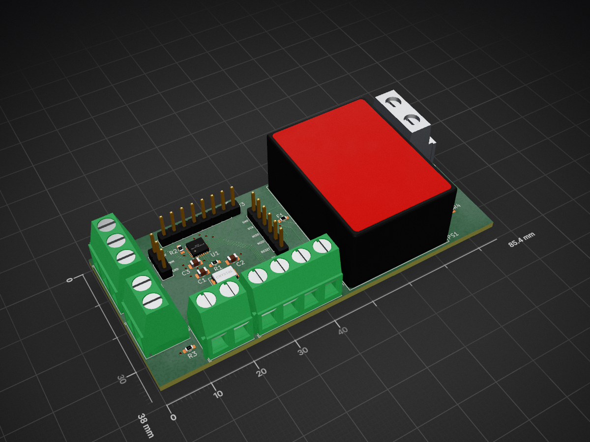
 George-P-1/Gate-Access-Control-PCB
KiCAD Designing (Schematic and PCB)
Gate Access Control is an open-source printed circuit board by George-P-1, from the George-P-1/Gate-Access-Control-PCB repository on GitHub. It is a 2-layer board of 85.4 × 38 mm with 20 parts on 30 nets, routed with 139 tracks and 13 vias.
It is built around the ATMEGA328-MMH. Its parts include 8 connectors, 4 resistors, 3 capacitors, 1 IC and 1 diode. It belongs with the AVR (ATmega, ATtiny) boards of this library.
A custom-designed PCB for a smart gate access control system, created using KiCad. It features both programming and power management components intended as part of a smart automation system for gates. This project was done as part of a university group assignment.
The system allows access via RF remote, switch or RFID tag and includes safety mechanisms like human detection inputs (photo sensors) that prevent gate operation. The board is designed to be AC-powered, with an onboard AC-DC converter and expansion-ready via various screw terminals and headers.
This project involved designing a custom PCB using KiCad 7, building the schematic and layout, selecting components and producing a bill of materials.
“Make a device that authenticates the opening of a gate using a remote, switch or RFID tag and opens the gate using a motor drive - unless two photo sensors detect a person near the gate.”
System Requirements:
Safety Considerations:
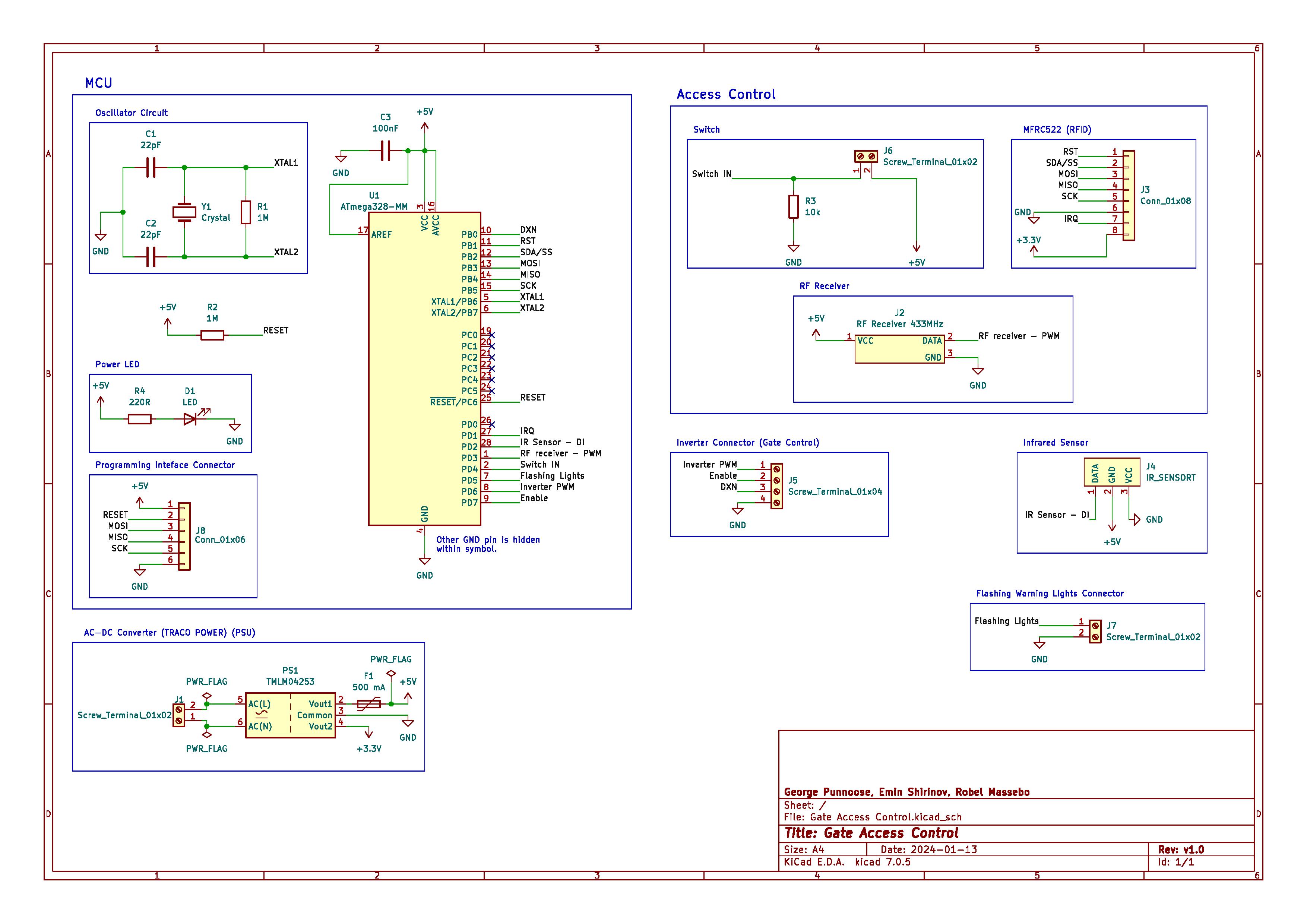 See pdf here for a detailed view.
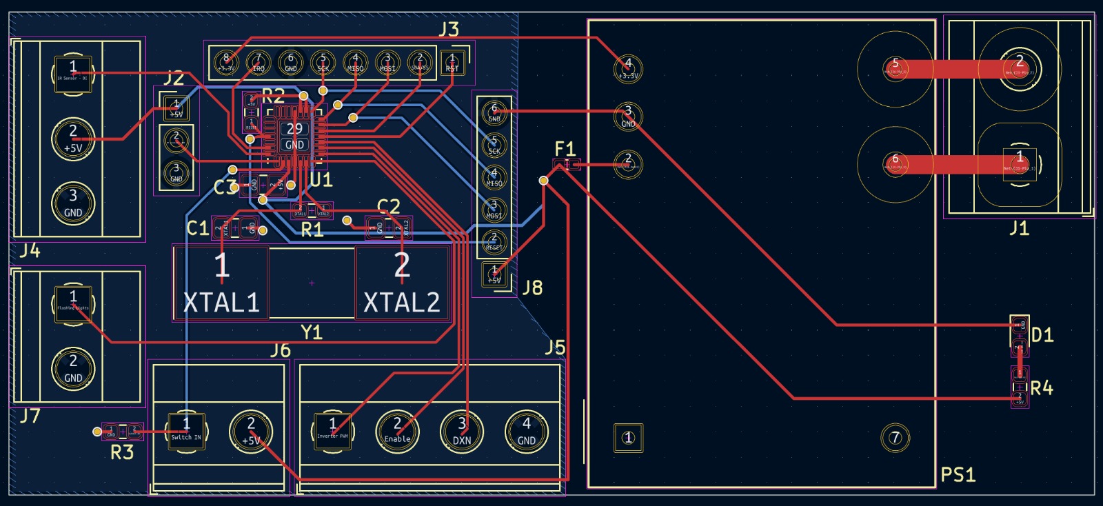
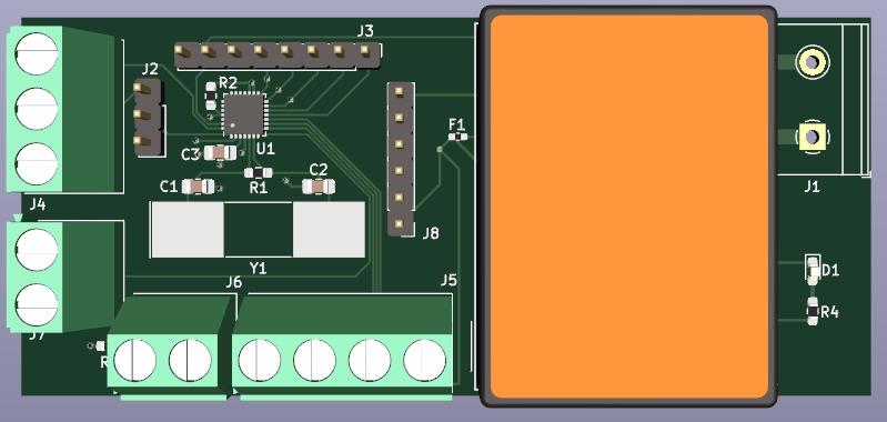
For detailed pricing and sourcing: See BOM PDF
Download CAM Files (Gerbers + Drill Maps)
These were used to estimate PCB production cost and can be uploaded to fabrication services (such as PCBway).
This project was developed for academic purposes and may require adaptation for industrial or commercial deployment.
| Qty | Value | Footprint | References |
|---|---|---|---|
| 2 | 1M | Resistor_SMD:R_0603_1608Metric_Pad0.98x0.95mm_HandSolder | R1, R2 |
| 2 | 22pF | Capacitor_SMD:C_0805_2012Metric_Pad1.18x1.45mm_HandSolder | C1, C2 |
| 2 | Screw_Terminal_01x02 | TerminalBlock_Phoenix:TerminalBlock_Phoenix_MKDS-1,5-2-5.08_1x02_P5.08mm_Horizontal | J6, J7 |
| 1 | 100nF | Capacitor_SMD:C_0805_2012Metric_Pad1.18x1.45mm_HandSolder | C3 |
| 1 | 10k | Resistor_SMD:R_0603_1608Metric_Pad0.98x0.95mm_HandSolder | R3 |
| 1 | 220R | Resistor_SMD:R_0603_1608Metric_Pad0.98x0.95mm_HandSolder | R4 |
| 1 | 500 mA | Fuse:Fuse_0603_1608Metric_Pad1.05x0.95mm_HandSolder | F1 |
| 1 | ATmega328-MM | Package_DFN_QFN:QFN-28-1EP_4x4mm_P0.45mm_EP2.4x2.4mm | U1 |
| 1 | Conn_01x06 | Connector_PinHeader_2.54mm:PinHeader_1x06_P2.54mm_Vertical | J8 |
| 1 | Conn_01x08 | Connector_PinHeader_2.54mm:PinHeader_1x08_P2.54mm_Vertical | J3 |
| 1 | Crystal | Crystal:Crystal_SMD_Abracon_ABM3-2Pin_5.0x3.2mm | Y1 |
| 1 | IR_SENSORT | TerminalBlock_Phoenix:TerminalBlock_Phoenix_MKDS-1,5-3-5.08_1x03_P5.08mm_Horizontal | J4 |
| 1 | LED | LED_SMD:LED_0603_1608Metric_Pad1.05x0.95mm_HandSolder | D1 |
| 1 | RF Receiver 433MHz | Connector_PinHeader_2.54mm:PinHeader_1x03_P2.54mm_Vertical | J2 |
| 1 | Screw_Terminal_01x02 | TerminalBlock_MetzConnect:TerminalBlock_MetzConnect_Type175_RT02702HBLC_1x02_P7.50mm_Horizontal | J1 |
| 1 | Screw_Terminal_01x04 | TerminalBlock_Phoenix:TerminalBlock_Phoenix_MKDS-1,5-4-5.08_1x04_P5.08mm_Horizontal | J5 |
| 1 | TMLM04253 | Converter_ACDC:Converter_ACDC_TRACO_TMLM-04_THT | PS1 |


atopile/atopile
Design circuit boards with code! ✨ Get software-like design reuse 🚀, validation, version control and collaboration in hardware; starting with electronics ⚡️

davidphilipbarr/Sweep
Sweep - a small promicro based keyboard inspired by the Ferris.

rusefi/rusefi
rusefi - GPL internal combustion engine control unit

hoglet67/RGBtoHDMI
Bare-metal Raspberry Pi project that provides pixel-perfect sampling of Retro Computer RGB/YUV video and conversion to HDMI
It measures 85.4 × 38 mm and has 2 copper layers, 1.59 mm thick.
20 parts, built around the ATMEGA328-MMH. The full list of its parts is on this page, with links to each part's symbol and footprint where PCBKit's library has them.
From the George-P-1/Gate-Access-Control-PCB repository on GitHub, at the commit this page was made from: the board is Gate Access Control.kicad_pcb and its schematic Gate Access Control.kicad_sch. PCBKit opens the board in the browser, with nothing to install.
Its repository states no licence, so its author keeps all rights: ask George-P-1 before reusing the design.