
4 layers60 × 60 mm
Rocket payload
Gupatron/Gupsfirstpcb
This is the first pcb that I will manufacture and intend to use for teleop usecases in my personal projects.
138 parts

 EzerLonginus/ESP32_S3_WROOM_Breakout
Breakout Board for ESP32 S3 WROOM
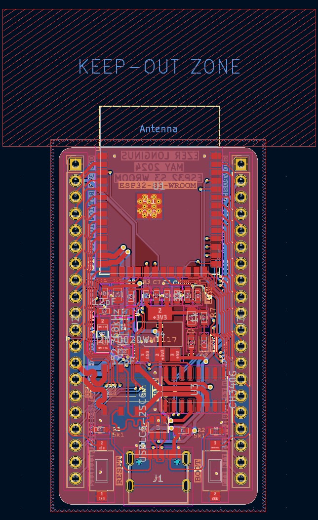
ESP32 S3 Breakout is an open-source printed circuit board by EzerLonginus, from the EzerLonginus/ESP32_S3_WROOM_Breakout repository on GitHub, published under the GPL-3.0 licence. It is a 2-layer board of 30.5 × 54.7 mm with 32 parts on 65 nets, routed with 844 tracks and 72 vias.
It is built around the ESP32-S3-WROOM-1-N8, CH340G and LM1117-3.3, with the USBLC6-2SC6 and 2N7002DW among its other parts. Its parts include 10 capacitors, 7 resistors, 4 ICs, 3 connectors and 3 switches. It belongs with the interfaces and adapters boards and the ESP32 boards of this library.


Breakout Board for ESP32 S3 WROOM
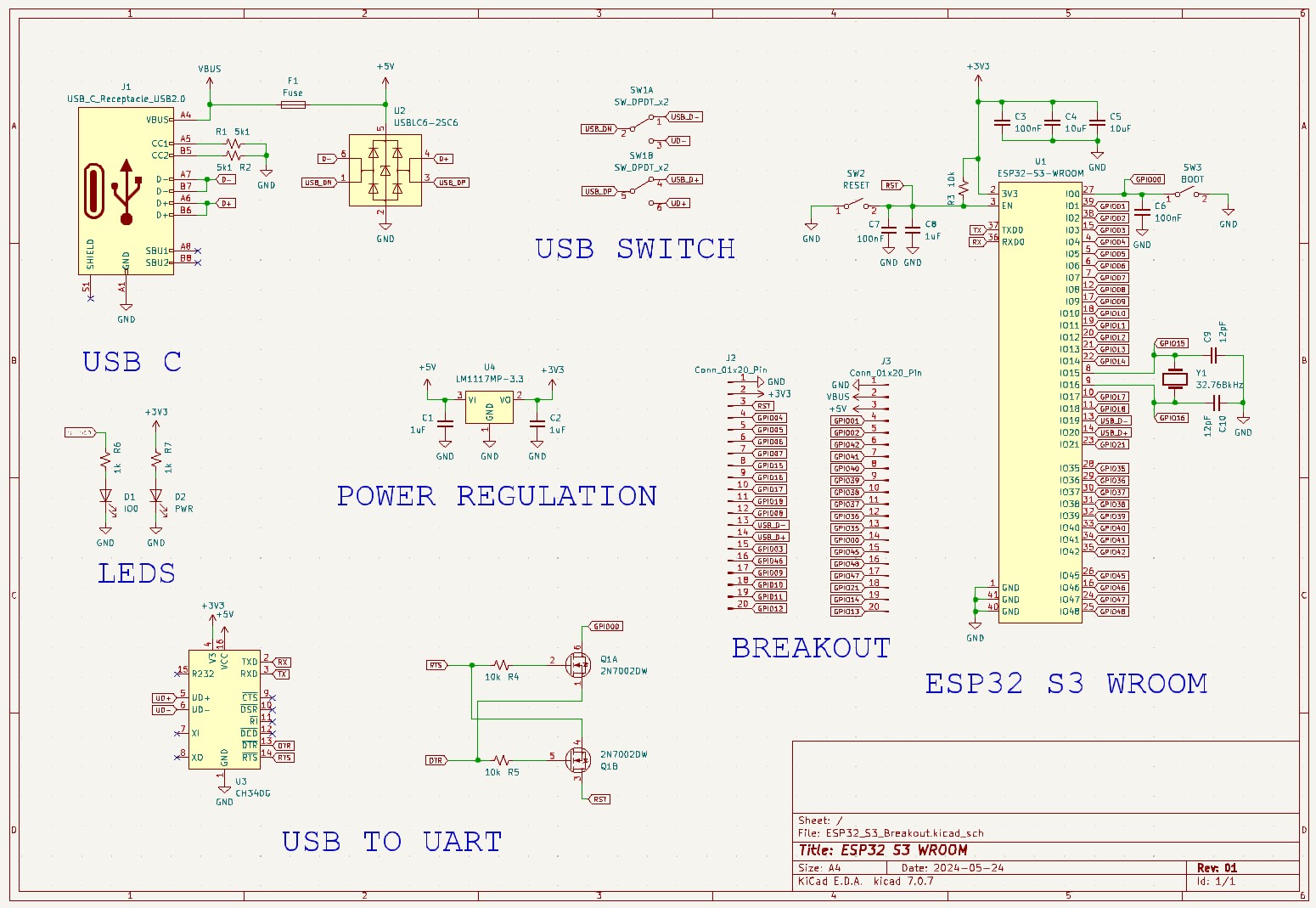
This board is a simple breakout for the ESP32 S3 WROOM. The interface includes the standard reset and boot button, with a USB to UART CH340G converter, and a 3V3 regulator. All GPIO pins are broken out to standard 2.54mm headers. USB-C reseptacle connector is used, but at the USB 2.0 standard.
This is mostly an excersize in designing an ESP32 module for inclusion in other projects. Once this design is functional, I'll start using it as a template for more custom oriented projects involving the chip (or some variant). I decided on the ESP S3 WROOM, because the S2 Solo seems to be slowly phasing out, and also doesn't have bluetooth functionality. Depending on how this excersize goes, I may start designing boards with just the bare chip (no built in WiFi antenna, SPI Flash, etc).
| Qty | Value | Footprint | References |
|---|---|---|---|
| 3 | 100nF | Capacitor_SMD:C_0603_1608Metric | C3, C6, C7 |
| 3 | 10k | Resistor_SMD:R_0603_1608Metric | R3, R4, R5 |
| 3 | 1uF | Capacitor_SMD:C_0603_1608Metric | C1, C2, C8 |
| 2 | 10uF | Capacitor_SMD:C_0805_2012Metric | C4, C5 |
| 2 | 12pF | Capacitor_SMD:C_0603_1608Metric | C9, C10 |
| 2 | 1k | Resistor_SMD:R_0603_1608Metric | R6, R7 |
| 2 | 5k1 | Resistor_SMD:R_0603_1608Metric | R1, R2 |
| 2 | Conn_01x20_Pin | Connector_PinHeader_2.54mm:PinHeader_1x20_P2.54mm_Vertical | J2, J3 |
| 1 | 2N7002DW | Package_TO_SOT_SMD:SOT-363_SC-70-6 | Q1 |
| 1 | 32.768kHz | Crystal:Crystal_SMD_EuroQuartz_EQ161-2Pin_3.2x1.5mm_HandSoldering | Y1 |
| 1 | BOOT | Button_Switch_SMD:SW_SPST_CK_RS282G05A3 | SW3 |
| 1 | CH340G | Package_SO:SOIC-16_3.9x9.9mm_P1.27mm | U3 |
| 1 | ESP32-S3-WROOM | RF_Module:ESP32-S3-WROOM-1 | U1 |
| 1 | Fuse | Fuse:Fuse_0603_1608Metric | F1 |
| 1 | IO0 | LED_SMD:LED_0603_1608Metric | D1 |
| 1 | LM1117 | Package_TO_SOT_SMD:SOT-223-3_TabPin2 | U4 |
| 1 | PWR | LED_SMD:LED_0603_1608Metric | D2 |
| 1 | RESET | Button_Switch_SMD:SW_SPST_CK_RS282G05A3 | SW2 |
| 1 | SW_DPDT_x2 | ELonginus:SMD DPDT Toggle SS-3235S-L1 | SW1 |
| 1 | USBLC6-2SC6 | Package_TO_SOT_SMD:SOT-23-6 | U2 |
| 1 | USB_C_Receptacle_USB2.0 | Connector_USB:USB_C_Receptacle_G-Switch_GT-USB-7010ASV | J1 |
Gupatron/Gupsfirstpcb
This is the first pcb that I will manufacture and intend to use for teleop usecases in my personal projects.

Omern187/lite-wing-drone
This repository contains the current KiCad-based LiteWing prototype package: source PCB files, manufacturing outputs, assembly data, 3D reference models, firmware binaries, datasheets, and design-review records.

ysaip07/KiCAD_Project
Personal PCB design projects using KiCad, reflecting a strong foundation in electronics design, component footprints, and PCB fabrication workflows.

tombueng/hilprobe
HILprobe: multi-function UUT probe for hardware-in-the-loop testing - RS-485, CAN FD, logic analyzer, 4-ch scope, two programmable UUT supplies. KiCad 10, 6 layers, RP2350B + ESP32-S3.


It measures 30.5 × 54.7 mm and has 2 copper layers, 1.6 mm thick.
32 parts, built around the ESP32-S3-WROOM-1-N8, CH340G, LM1117-3.3 and USBLC6-2SC6. The full list of its parts is on this page, with links to each part's symbol and footprint where PCBKit's library has them.
From the EzerLonginus/ESP32_S3_WROOM_Breakout repository on GitHub, at the commit this page was made from: the board is hardware/ESP32_S3_Breakout/ESP32_S3_Breakout.kicad_pcb and its schematic hardware/ESP32_S3_Breakout/ESP32_S3_Breakout.kicad_sch. PCBKit opens the board in the browser, with nothing to install.
Its repository publishes it under the GPL-3.0 licence: you may reuse it on that licence's terms (keep the author's notice, and for a copyleft licence share your changes alike).