2 layers40 × 34 mm
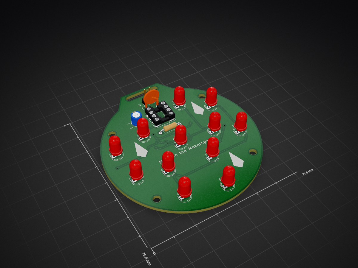
 Electro707/2019_Ornament_PCB_Kit
A PCB Kit in the shape of an ornament
2019 Ornament PCB Kit is an open-source printed circuit board by Electro707, from the Electro707/2019_Ornament_PCB_Kit repository on GitHub. It is a 2-layer board of 30 × 40 mm with 37 parts on 19 nets, routed with 161 tracks and 11 vias.
Its parts include 13 resistors, 12 diodes, 2 capacitors, 1 IC and 1 connector.
A PCB Kit in the shape of an ornament
This repository is archived, as it's a one-time design. Now files are hosted on Google Drive.
Link to website, in which the Google Drive link can be found: Link
I may create a new general reposity for the kit that will be updated as time goes on (there also won't be any of the University of New Haven logos on that one).
| Qty | Value | Footprint | References |
|---|---|---|---|
| 12 | 68 | Resistor_SMD:R_1206_3216Metric_Pad1.42x1.75mm_HandSolder | R1, R2, R3, R4, R5, R6, R7, R8, R9, R10, R11, R12 |
| 12 | LED_ALT | LED_THT:LED_D5.0mm | D1, D2, D3, D4, D5, D6, D7, D8, D9, D10, D11, D12 |
| 4 | M3 Mounting Hole | MountingHole:MountingHole_3.2mm_M3_DIN965 | H1, H2, H3, H4 |
| 2 | SolderJumper_3_Bridged12 | Jumper:SolderJumper-3_P1.3mm_Bridged12_Pad1.0x1.5mm | JP1, JP2 |
| 1 | 1uF | Capacitor_SMD:C_1206_3216Metric_Pad1.42x1.75mm_HandSolder | C2 |
| 1 | Battery | Connector_PinHeader_2.54mm:PinHeader_1x02_P2.54mm_Vertical | J1 |
| 1 | C | Capacitor_THT:CP_Radial_D5.0mm_P2.50mm | C1 |
| 1 | LM555 | Package_DIP:DIP-8_W7.62mm_Socket_LongPads | U1 |
| 1 | LOGO | Logo:UNH 13.4x13.4 | G*** |
| 1 | Polyfuse | Fuse:Fuse_BelFuse_0ZRE0005FF_L8.3mm_W3.8mm | F1 |
| 1 | R | Resistor_THT:R_Axial_DIN0207_L6.3mm_D2.5mm_P10.16mm_Horizontal | R13 |

hoglet67/RGBtoHDMI
Bare-metal Raspberry Pi project that provides pixel-perfect sampling of Retro Computer RGB/YUV video and conversion to HDMI

hackclub/OnBoard
💡 Join 1,000 teenagers and make your first PCB with a $100 grant!

FreeYourStream/freedeck-hardware
all the stuff you need to build your own FreeDeck

stuartpittaway/diyBMS
Do it yourself battery management system for Lithium ion battery packs/cells

Pwnsat/FlatSat
Flatsat v1.0 is a hardware based platform for aerospace cybersecurity research


vsfteam/vsf
Versaloon Software Framework -- a tiny preemptive-capable event-driven incremental software framework for embedded systems
It measures 30 × 40 mm and has 2 copper layers, 1.6 mm thick.
37 parts. The full list of its parts is on this page, with links to each part's symbol and footprint where PCBKit's library has them.
From the Electro707/2019_Ornament_PCB_Kit repository on GitHub, at the commit this page was made from: the board is KiCad Files/PCB.kicad_pcb. PCBKit opens the board in the browser, with nothing to install.
Its repository states no licence, so its author keeps all rights: ask Electro707 before reusing the design.