2 layers70.4 × 48.2 mm

 CGrassin/microscope_led_light_circuit2
A dimming LED circuit designed for optical microscopes.
Microscope LED is an open-source printed circuit board by CGrassin, from the CGrassin/microscope_led_light_circuit repository on GitHub, published under the CC-BY-4.0 licence. It is a 2-layer board of 40 × 21.1 mm with 20 parts on 21 nets, routed with 88 tracks and 10 vias.
It is built around the NE555, AO3400A and XT30PW-F. Its parts include 6 resistors, 4 capacitors, 2 diodes, 2 connectors and 1 IC.


This circuit drives a 1W or 3W LED to convert old optical microscopes from light bulb/halogen lamp to LED ligthing.
It is powered from a USB type C port and is fully dimmable. It may be used with a USB power bank, for instance.
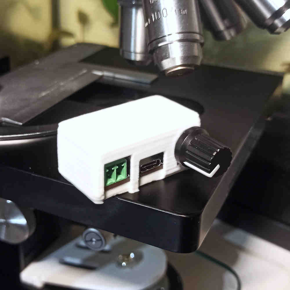
LEDs are considerably more efficient (i.e. less heat), have a longer lifespan and have a better color accuracy than bulbs. My circuit has a high PWM frequency to avoid flickering and rolling bands effect in photographs.
| Specification | Value |
|---|---|
| Power input | 5V @ 1A max. (USB type C) |
| PWM frequency | >8KHz |
| Controls | Combined knob dimming (0-100%) and ON/OFF |
| Estimated cost | About $10 |
Gerber files are ready to upload to your prefered PCB manufacturer. The components are generic and should be available at most electronic components distributors. I personally use JLCPCB and LCSC.
Hand soldering this board is easy. I included an "interactive BOM" to help with part placement.
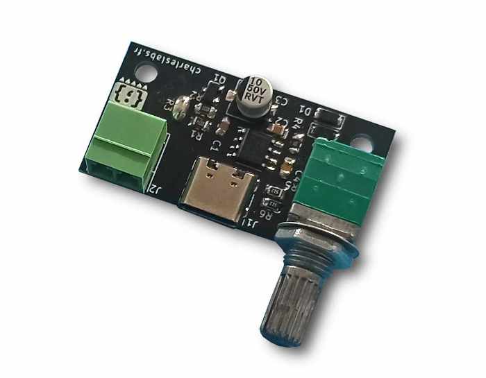
The only additional required parts are a 1W or 3W "star" LED with a 30° lens to pre-focus the light into the condenser. Thank to this lens, a 1W LED is sufficient. You can choose your favorite color temperature.
I also included a 3D-printable case for the circuit. Print at 0.2mm layer height, no support required.
Although I designed a PCB, this circuit could be build on a piece of stripboard or even breadboard.
This circuit uses a classic 555 variable duty cycle astable multivibrator configuration.
The potentiometer adjusts the charge and discharge rate of the TRIG capacitor. The frequency of the carrier depend on the RC constant of those parts.
All files in this repository are released under CC-BY license.
| Qty | Value | Footprint | References |
|---|---|---|---|
| 2 | 100n | Capacitor_SMD:C_0805_2012Metric_Pad1.15x1.40mm_HandSolder | C2, C4 |
| 2 | 4007 | Diode_SMD:D_SOD-123F | D1, D2 |
| 2 | 5.1k | Resistor_SMD:R_0805_2012Metric_Pad1.15x1.40mm_HandSolder | R5, R6 |
| 2 | MountingHole | MountingHole:MountingHole_3.2mm_M3 | H1, H2 |
| 1 | 100 | Resistor_SMD:R_0805_2012Metric_Pad1.15x1.40mm_HandSolder | R1 |
| 1 | 10u | Capacitor_SMD:CP_Elec_5x5.4 | C3 |
| 1 | 1M | Resistor_SMD:R_0805_2012Metric_Pad1.15x1.40mm_HandSolder | R2 |
| 1 | 22 | Resistor_SMD:R_1206_3216Metric | R3 |
| 1 | 22n | Capacitor_SMD:C_0805_2012Metric_Pad1.15x1.40mm_HandSolder | C1 |
| 1 | 510 | Resistor_SMD:R_0805_2012Metric_Pad1.15x1.40mm_HandSolder | R4 |
| 1 | 5k (RV097) | C10418:RV097 | RV1 |
| 1 | AO3400A | Package_TO_SOT_SMD:SOT-23 | Q1 |
| 1 | Logo_Open_Hardware_Large | Charleslabs_Parts:Charleslabs_Logo_5mm | LOGO1 |
| 1 | NE555 | Package_SO:SOIC-8_3.9x4.9mm_P1.27mm | U1 |
| 1 | USB_C_Receptacle | Connector_USB:USB_C_Receptacle_HRO_TYPE-C-31-M-12 | J1 |
| 1 | XT30PW-F | Connector_Phoenix_MC:PhoenixContact_MC_1,5_2-G-3.81_1x02_P3.81mm_Horizontal | J2 |

telagod/moskill
MosKill - Smart Mosquito Swatter with BLE, Kill Counting & Statistics | ESP32-C3 + KiCad PCB + UniApp


Arrow-air/project-quiver
Project Quiver documentation, designs, and project artifacts.

Kelvin-Ziqi-Zhao/drone-current-sensor-board
High current sensor board for battery+capacitor power supply system

ThunderFly-aerospace/TFSBEC01
High efficient switching power supply for UAV actuators.

It measures 40 × 21.1 mm and has 2 copper layers, 1.6 mm thick.
20 parts, built around the NE555, AO3400A and XT30PW-F. The full list of its parts is on this page, with links to each part's symbol and footprint where PCBKit's library has them.
From the CGrassin/microscope_led_light_circuit repository on GitHub, at the commit this page was made from: the board is Microscope_LED_circuit/Microscope_LED.kicad_pcb. PCBKit opens the board in the browser, with nothing to install.
Its repository publishes it under the CC-BY-4.0 licence: you may reuse it on that licence's terms (keep the author's notice, and for a copyleft licence share your changes alike).