2 layers85 × 85 mm
 Bulldogs-Racing/HV-PCB
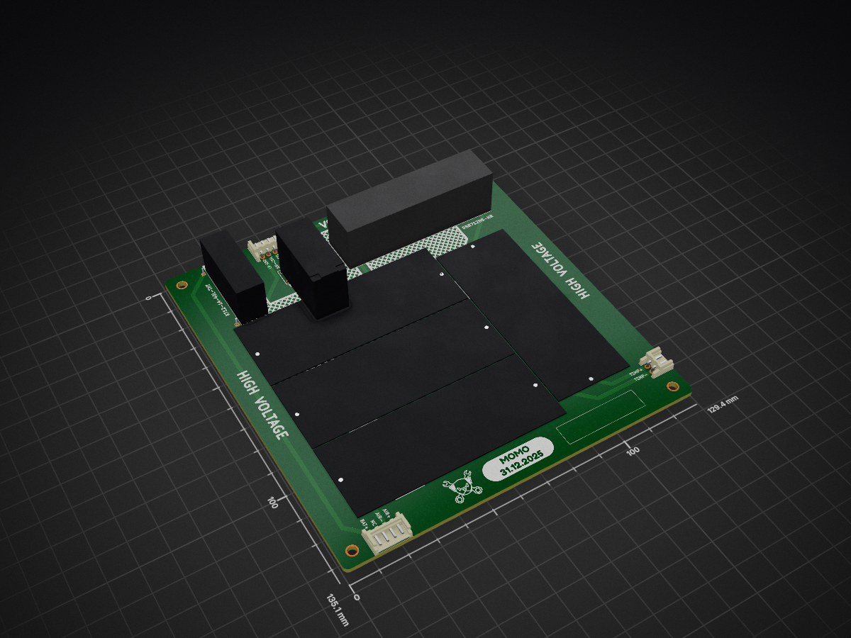
HV PCB redesign is an open-source printed circuit board by Bulldogs-Racing, from the Bulldogs-Racing/HV-PCB repository on GitHub. It is a 2-layer board of 129.4 × 135.1 mm with 18 parts on 14 nets, routed with 45 tracks and 0 vias.
It is built around the DBR71205-HR, KT12-1A-40L-THT and TSC-112L3H,000.

| Qty | Value | Footprint | References |
|---|---|---|---|
| 4 | PCBMH3, PCBMH3, PCBMH4, PCBMH5 | ||
| 3 | LOGO | LOGO | G***, G***, G*** |
| 2 | 10k | Resistor_THT:UAL50-5KF8 | TSMP-_Res1, TSMP+_Res1 |
| 2 | JST_2.50_Horizontal | Connector_JST:JST_EH_S4B-EH_1x04_P2.50mm_Horizontal | HV_Conn1, LV_Conn1 |
| 1 | 1.5k | Resistor_THT:UAL50-5KF8 | Precharge_Res1 |
| 1 | 5k | Resistor_THT:UAL50-5KF8 | Discharge_Res1 |
| 1 | DBR71205-HR | Relay_SMD:DBR71205HR | Discharge_Relay1 |
| 1 | G*** | kibuzzard-69545008 | kibuzzard-69545008 |
| 1 | JST_2.50_Horizontal | Connector_JST:JST_EH_S2B-EH_1x02_P2.50mm_Horizontal | TSMP_Conn1 |
| 1 | KT12-1A-40L-THT | Relay_SMD:RELAY_KT12-1A-40L-THT | Precharge_Relay1 |
| 1 | TSC-112L3H,000 | Relay_SMD:TSC105D3H000 | Precharge_Control1 |


VoronDesign/Voron-Hardware
Cool Hardware designed by the Voron Design group


hackclub/OnBoard
💡 Join 1,000 teenagers and make your first PCB with a $100 grant!

VoronDesign/Voron-Tap
Tap is a nozzle-based z-probe for the V2 and Trident printer designs. The entire toolhead moves to trigger an optical switch. Tap offers many advantages:

Luos-io/luos_engine
Open-source and real-time orchestrator for cyber-physical-systems, to easily design, test and deploy embedded applications and digital twins.
It measures 129.4 × 135.1 mm and has 2 copper layers, 1.81 mm thick.
18 parts, built around the DBR71205-HR, KT12-1A-40L-THT and TSC-112L3H,000. The full list of its parts is on this page, with links to each part's symbol and footprint where PCBKit's library has them.
From the Bulldogs-Racing/HV-PCB repository on GitHub, at the commit this page was made from: the board is HV PCB redesign.kicad_pcb and its schematic HV PCB redesign.kicad_sch. PCBKit opens the board in the browser, with nothing to install.
Its repository states no licence, so its author keeps all rights: ask Bulldogs-Racing before reusing the design.