
2 layers297.2 × 180.3 mm

 Beaupre-Circuit-Design/23xx-Adapter3
Adapter for using a standard JDEC 28/32 pin EPROM/EEPROM to replace a 23xx Rom
23xx Adapter is an open-source printed circuit board by Beaupre-Circuit-Design, from the Beaupre-Circuit-Design/23xx-Adapter repository on GitHub, published under the MIT licence. It is a 4-layer board of 19.7 × 41.9 mm with 41 parts on 44 nets, routed with 322 tracks and 25 vias.
It is built around the 74HCT138D. Its parts include 8 resistors and 2 ICs. It belongs with the interfaces and adapters boards of this library.
This is a rework of the excellent design made by Jim Brain to replace a 23xx ROM with a standard JEDEC 28 or 32 pin EPROM/EEPROM or Flash ROM. The main difference, this version is 1.9mm smaller in width and more centered on the socket, allowing enough spacing to replace all three roms in a C64 long-board version where Jim's is a little bit too large to install two side by side.
Since 23xx ROMs can be produced with active high or low select lines, the adapter can decode theses signals and select the ROM on the right one. Also the highest address lines not used by the original ROM are available via SMT pads for permanent configuration, or headers to allow bank dynamic bank switching.
The onboard 74HCT138 3-to-8 decoder converts any combination of the 3 possible chip select lines into a single JEDEC standard select line. If a select line is not needed, that input can be tied to ground via SMT pads on the bottom of the PCB.
| Pad | Position | |
|---|---|---|
| 18 | 1-2 | Line is routed to adress line A11, SMT Pad A should be solder close |
| 18 | 2-3 | Line is used as chip select, A11 can be drive by the SMT Pad or header |
| 20 | 1-2 | Line is routed to OE |
| 20 | 2-3 | Line is used as chip select |
| 21 | 1-2 | Line is routed to adress line A12, SMT Pad C should be solder close |
| 20 | 2-3 | Line is used as chip select, A12 can be drive by the SMT Pad or header |
Once configured, the following truth table show all the possible output at SMT Pads 0-7, solder the pad that is low when the original chip is selected.
| 18 | 20 | 21 | 0 | 1 | 2 | 3 | 4 | 5 | 6 | 7 |
|---|---|---|---|---|---|---|---|---|---|---|
| L | L | L | L | H | H | H | H | H | H | H |
| H | L | L | H | L | H | H | H | H | H | H |
| L | H | L | H | H | L | H | H | H | H | H |
| H | H | L | H | H | H | L | H | H | H | H |
| L | L | H | H | H | H | H | L | H | H | H |
| H | L | H | H | H | H | H | H | L | H | H |
| L | H | H | H | H | H | H | H | H | L | H |
| H | H | H | H | H | H | H | H | H | H | L |
| IC Model | Notes | A | B | C | 18 | 20 | 21 | 0 | 1 | 2 | 3 | 4 | 5 | 6 | 7 | |
|---|---|---|---|---|---|---|---|---|---|---|---|---|---|---|---|---|
| 2316 | !CS1, !CS2, CS3 | 2-3 | 2-3 | 2-3 | X | 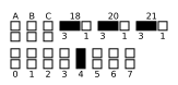 | ||||||||||
| 2716 | !EP, !G, Vpp | 2-3 | 2-3 | 2-3 | X | 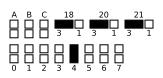 | ||||||||||
| 2332 | !CS1, CS2 | X | 1-2 | 2-3 | 2-3 | X | 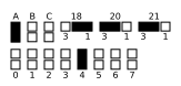 | |||||||||
| 2364 | !CS1 | X | X | 1-2 | 2-3 | 1-2 | X | 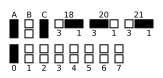 | ||||||||
| 2364 | !CS1 (Alt, no 74LS138 decoding) | 1-2 | 1-2 | 1-2 | 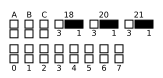 | |||||||||||
| 2364 | CS1 | X | X | 1-2 | 2-3 | 1-2 | X | 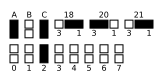 |
Do not forget to pull-up the WE pin or you risk overwriting your EEPROM. As example if using a 28C64/256, solder pad A14, or for 28C512/010/040, solder pad A18.
Depending on the size of the original and replacement rom, address lines 11 to 18 are available for bank switching, eiter by solder pads or using the 1.27mm header as shown in the pictures below.
| Solder Pads | 1.27mm Header |
|---|---|
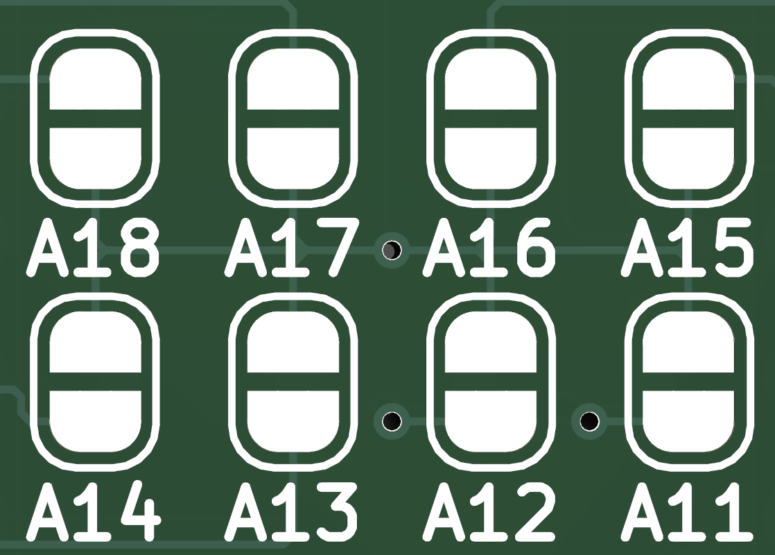 | 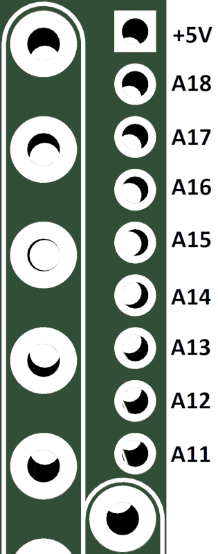 |
Gerbers files and SMD assembly files are available for uploading to your prefered manufacturer (I personnally use JLCPCB). The PCB use SMT parts, except for the headers) while the control board use through-hole components. Refer to the Bill of Materials Excel sheet for a complete list of needed components.
This work is licensed under the Creative Commons Attribution-NonCommercial-ShareAlike 4.0 International License. To view a copy of this license, visit http://creativecommons.org/licenses/by-nc-sa/4.0/ or send a letter to Creative Commons, PO Box 1866, Mountain View, CA 94042, USA.
| Revision | Description |
|---|---|
| 1.0 | Initial prototype |
| 2.0 | Add bank switching header |
| Qty | Value | Footprint | References |
|---|---|---|---|
| 20 | SolderJumper_2_Open | Jumper:SolderJumper-2_P1.3mm_Open_RoundedPad1.0x1.5mm | A11, A12, A13, A14, A15, A16, A17, A18, CF0, CF1, CF2, CF3, CF4, CF5, CF6, CF7 +4 |
| 8 | 10KΩ | Resistor_SMD:R_0603_1608Metric | R1, R2, R3, R4, R5, R6, R7, R8 |
| 3 | SolderJumper_3_Open | Jumper:SolderJumper-3_P1.3mm_Open_RoundedPad1.0x1.5mm_NumberLabels | CF18, CF20, CF21 |
| 1 | 74HCT138 | Package_SO:SOIC-16_3.9x9.9mm_P1.27mm | U2 |
| 1 | BCD_Logo | BeaupreCircuitDesign:BCD_Logo_5mm | G1 |
| 1 | ChickenLips | BeaupreCircuitDesign:ChickenLips_2.5mm | G2 |
| 1 | CreativeCommons | Creative_Common:CreativeCommons_2.5mm | G4 |
| 1 | CreativeCommons_Attribution | Creative_Common:CreativeCommons_Attribution_2.5mm | G6 |
| 1 | CreativeCommons_NonCommercial | Creative_Common:CreativeCommons_NonCommercial_2.5mm | G5 |
| 1 | CreativeCommons_ShareAlike | Creative_Common:CreativeCommons_ShareAlike_2.5mm | G7 |
| 1 | MOS_23xx_to_27xxx | MOS_23xx:MOS_23xx_to_27xxx | U1 |
| 1 | OpenSource_Hardware | BeaupreCircuitDesign:Open_Source_Hardware_2.5mm | G3 |
| 1 | Skull | BeaupreCircuitDesign:Skull_2.5mm | G8 |


leomil72/LM80C
A Z80-based homebrew computer withTMS9918, AY-3-8910, Z80 CTC, Z80 PIO, and Z80 SIO

DoctorWkt/CSCvon8
A crazy small 8-bit CPU built with only seventeen 7400-series chips.

electrified/rc2014-ym2149
KiCad schematics and gerbers for a YM sound card for the RC2014. See it in action here: https://www.youtube.com/watch?v=-iLwi9FagFE


It measures 19.7 × 41.9 mm and has 4 copper layers, 1.59 mm thick.
41 parts, built around the 74HCT138D. The full list of its parts is on this page, with links to each part's symbol and footprint where PCBKit's library has them.
From the Beaupre-Circuit-Design/23xx-Adapter repository on GitHub, at the commit this page was made from: the board is Kicad/23XX-Adapter.kicad_pcb and its schematic Kicad/23XX-Adapter.kicad_sch. PCBKit opens the board in the browser, with nothing to install.
Its repository publishes it under the MIT licence: you may reuse it on that licence's terms (keep the author's notice, and for a copyleft licence share your changes alike).