2 layers45.5 × 42.9 mm
Esphome han reader
hackclub/OnBoard
💡 Join 1,000 teenagers and make your first PCB with a $100 grant!
21 parts915

 AyushShuklaaa7/USB3_Ethernet_Interface
High-speed USB 3.1 Gen 1 to Gigabit Ethernet interface PCB designed in KiCad using the Microchip LAN7801 and KSZ9031RNX.
USB3 ethernet is an open-source printed circuit board by AyushShuklaaa7, from the AyushShuklaaa7/USB3_Ethernet_Interface repository on GitHub, published under the MIT licence. It is a 4-layer board of 81.9 × 35.3 mm with 81 parts on 87 nets, routed with 892 tracks and 155 vias.
It is built around the KSZ9031RNXCA, TLV1117LV33DCYT and ABM8G-25.000MHZ-B4Y-T, with the DMG2301L among its other parts. Its parts include 34 capacitors, 30 resistors, 4 ICs, 1 diode and 1 transistor. It belongs with the interfaces and adapters boards of this library.


This project is a hardware implementation of a USB 3.1 Gen 1 to Gigabit Ethernet adapter designed in KiCad. It is based on the Microchip LAN7801 USB-to-Ethernet controller and the KSZ9031RNX Gigabit Ethernet PHY.
The goal of this project was to gain practical experience in designing a high-speed PCB while following signal integrity, power integrity, and layout guidelines required for USB 3.1 and Gigabit Ethernet interfaces.
The LAN7801 acts as the USB 3.1 Gen 1 bridge and Ethernet MAC, converting 5 Gbps USB SuperSpeed data into a 125 MHz RGMII interface. The KSZ9031RNX then converts the RGMII data into standard Gigabit Ethernet signals that are transmitted through the RJ45 MagJack.
The design uses dedicated 3.3V and 1.2V power rails. Instead of using an external 1.2V regulator, the KSZ9031RNX's integrated LDO controller is used with a DMG2301L P-channel MOSFET to generate the PHY core supply, reducing the overall component count.
A 25 MHz ABM8G crystal provides the reference clock for both devices.
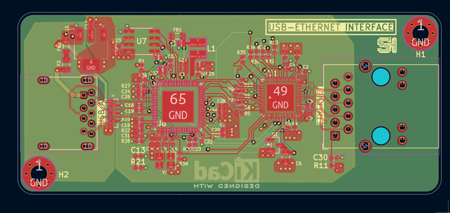
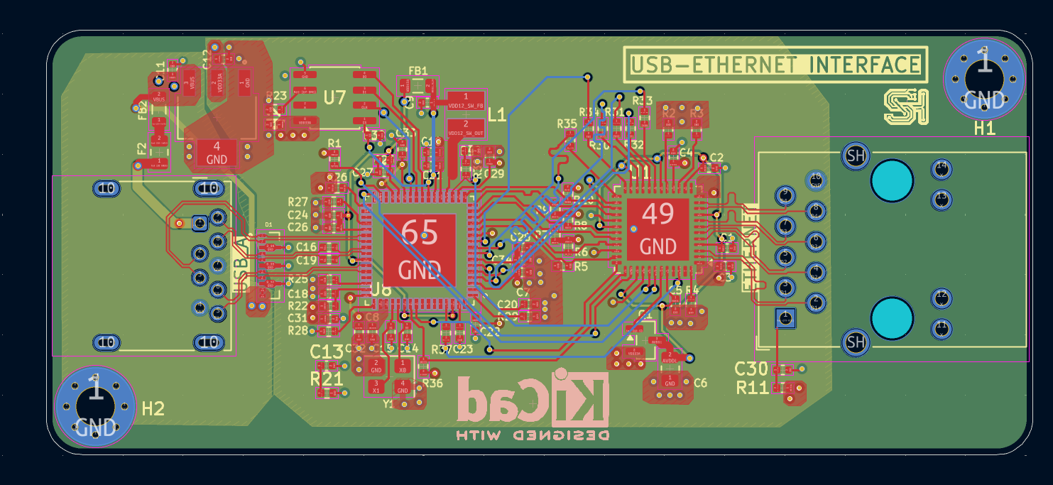
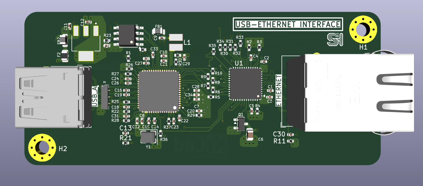
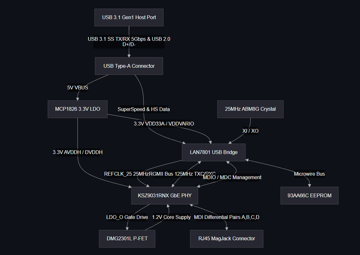
The USB Type-A connector interfaces with the LAN7801 controller. The controller communicates with the KSZ9031RNX Gigabit PHY over the RGMII interface, while MDIO/MDC is used for PHY configuration. The PHY then drives the RJ45 MagJack to provide a standard Gigabit Ethernet connection.
The project started by studying the LAN7801 and KSZ9031RNX datasheets along with the manufacturer's reference designs to understand the required interfaces, power supplies, clocking, and layout recommendations.
After completing the schematic, component placement was planned carefully to keep high-speed signal paths as short as possible. The USB controller was placed close to the USB connector, while the Ethernet PHY was positioned near the RJ45 MagJack to minimize RGMII routing.
During PCB layout, the main focus was maintaining signal integrity by following controlled impedance routing, differential pair routing, length matching, proper grounding, and good decoupling practices.
| Component | Description |
|---|---|
| LAN7801 | USB 3.1 Gen 1 to Gigabit Ethernet Controller |
| KSZ9031RNX | Gigabit Ethernet PHY |
| ABM8G | 25 MHz Crystal Oscillator |
| DMG2301L | P-Channel MOSFET |
| RJ45 MagJack | Gigabit Ethernet Connector |
| USB Type-A Connector | USB SuperSpeed Interface |
Some of the key challenges while designing this PCB were:
Ayush Shukla
B.Tech Electronics & Telecommunication Engineering
| Qty | Value | Footprint | References |
|---|---|---|---|
| 16 | 0.1uF | Capacitor_SMD:C_0402_1005Metric | C7, C8, C13, C16, C17, C19, C21, C24, C25, C27, C28, C29, C31, C32, C33, C34 |
| 8 | 4.7K | Resistor_SMD:R_0402_1005Metric | R2, R3, R5, R6, R7, R8, R9, R10 |
| 7 | 100nF | Capacitor_SMD:C_0402_1005Metric | C1, C2, C3, C4, C5, C18, C30 |
| 7 | 22R | Resistor_SMD:R_0402_1005Metric | R30, R31, R32, R33, R34, R35, R37 |
| 6 | 10K | Resistor_SMD:R_0402_1005Metric | R1, R23, R25, R26, R38, R40 |
| 4 | 1uF | Capacitor_SMD:C_0402_1005Metric | C11, C22, C23, C26 |
| 2 | 12K | Resistor_SMD:R_0402_1005Metric | R4, R28 |
| 2 | 15pF | Capacitor_SMD:C_0402_1005Metric | C14, C15 |
| 2 | MountingHole_Pad | MountingHole:MountingHole_3.2mm_M3_Pad_Via | H1, H2 |
| 1 | 0.1uF | Resistor_SMD:R_0402_1005Metric | R29 |
| 1 | 0483930003 | Connector_USB:USB3_A_Molex_48393-001 | USB_A |
| 1 | 0R | Resistor_SMD:R_0402_1005Metric | R39 |
| 1 | 100K | Resistor_SMD:R_0402_1005Metric | R22 |
| 1 | 10k | Resistor_SMD:R_0402_1005Metric | R27 |
| 1 | 10uF | Capacitor_SMD:C_0805_2012Metric | C6 |
| 1 | 10uF | Capacitor_SMD:C_0402_1005Metric | C12 |
| 1 | 1K | Resistor_SMD:R_0402_1005Metric | R36 |
| 1 | 220R | Inductor_SMD:L_0805_2012Metric | FB1 |
| 1 | 22uF | Capacitor_SMD:C_0402_1005Metric | C9 |
| 1 | 2K | Capacitor_SMD:C_0402_1005Metric | C20 |
| 1 | 3.3uH | ME3220-102MLB:IND_ME3220-102MLB | L1 |
| 1 | 330k | Resistor_SMD:R_0402_1005Metric | R21 |
| 1 | 4.7uF | Capacitor_SMD:C_0402_1005Metric | C10 |
| 1 | 75R | Resistor_SMD:R_0402_1005Metric | R11 |
| 1 | 93AAxxC | Package_SO:SOIC-8_3.9x4.9mm_P1.27mm | U7 |
| 1 | ABM8G-25.000MHZ-B4Y-T | Crystal:Crystal_SMD_Abracon_ABM8G-4Pin_3.2x2.5mm | Y1 |
| 1 | DMG2301L | Package_TO_SOT_SMD:SOT-23 | Q1 |
| 1 | ESD8008MUTAG | ESD8008MUTAG:DIO_ESD8008MUTAG | D1 |
| 1 | FerriteBead | Inductor_SMD:L_0805_2012Metric | FB2 |
| 1 | KSZ9031RNXCA | Package_DFN_QFN:QFN-48-1EP_7x7mm_P0.5mm_EP5.15x5.15mm | U1 |
| 1 | LAN7801-I_9JX | LAN7801-I_9JX:QFN50P900X900X100-65N_LAN7801-I_9JX | U8 |
| 1 | LOGO | N_logo:sh_sh | G*** |
| 1 | Polyfuse | Fuse:Fuse_0805_2012Metric | F2 |
| 1 | TLV1117LV33DCYT | TLV1117LV33DCYT:SOT230P700X180-4N | U2 |
| 1 | WE-RJ45_7499111446 | Connector_RJ:RJ45_Wuerth_7499111446_Horizontal | ETHERNET |
The 80 most common of 81 parts.
hackclub/OnBoard
💡 Join 1,000 teenagers and make your first PCB with a $100 grant!


filliformes/pandore
pandore is an open-source digital audio instrument protyping platform based on the LattePanda Mu.

ngrabbs/ember
Open pvpanel.kicadpro with KiCad 10. The project contains the recovered schematic, routed PCB, project-local footprint libraries, and solar-module STEP model.


SamuelCicuitStudio/LAN9645-STM32-Managed-Ethernet-Switch
Managed Ethernet switch platform built around the LAN9645 and STM32H743, featuring copper and SerDes ports, SPI management, RMII, LwIP, and a USB diagnostic CLI.


antmicro/artix-dc-scm
Experimental Xilinx Artix-7 driven Data Center Security Communication Module
It measures 81.9 × 35.3 mm and has 4 copper layers, 1.59 mm thick.
81 parts, built around the KSZ9031RNXCA, TLV1117LV33DCYT, ABM8G-25.000MHZ-B4Y-T and DMG2301L. The full list of its parts is on this page, with links to each part's symbol and footprint where PCBKit's library has them.
From the AyushShuklaaa7/USB3_Ethernet_Interface repository on GitHub, at the commit this page was made from: the board is USB3_ethernet.kicad_pcb and its schematic POWER.kicad_sch. PCBKit opens the board in the browser, with nothing to install.
Its repository publishes it under the MIT licence: you may reuse it on that licence's terms (keep the author's notice, and for a copyleft licence share your changes alike).