4 layers76 × 46 mm
Board f
Alfredapp-hash/Guardian_One
Nets listed on the optional .kicadpcb shell match this table.
25 parts
 Alfredapp-hash/Guardian_One
Nets listed on the optional .kicadpcb shell match this table.
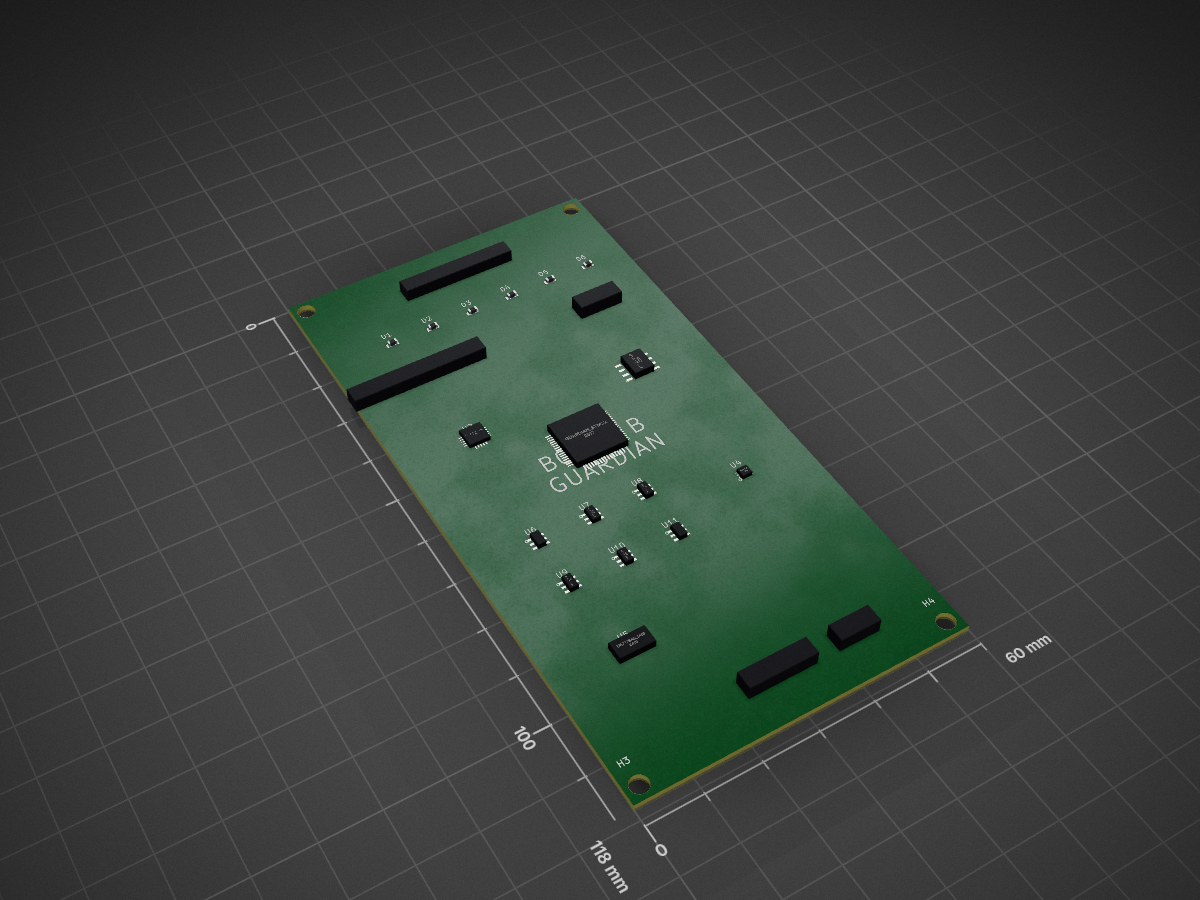
Board b is an open-source printed circuit board by Alfredapp-hash, from the Alfredapp-hash/Guardian_One repository on GitHub. It is a 6-layer board of 60 × 118 mm with 28 parts on 13 nets.
Its parts include 11 ICs, 6 diodes and 4 connectors. It belongs with the STM32 boards of this library.
| Field | Value |
|---|---|
| Date | 2026-07-30 |
| Status | Docs + optional KiCad shell — not fab-ready |
| Outline | 40 × 60 mm |
| Purpose | Heater / SoC simulator stack carrier for bench thermal mock |
gerbers/ folder. Author schematic/PCB fully in KiCad, then export.Provide a small FR4 carrier that:
| Conn | Net | Function |
|---|---|---|
| J1-1 | HEATER_5V | Heater supply (+5 V from lab PSU) |
| J1-2 | GND | Heater return |
| J2-1 | NTC_HEATER | Probe at heater |
| J2-2 | NTC_VC | Probe at VC inlet |
| J2-3 | NTC_SPINE | Graphite mid-spine |
| J2-4 | NTC_REAR | Rear thermal window |
| J2-5 | NTC_RAIL | Side rail |
| J2-6 | NTC_AMB | Ambient |
| J2-7 | NTC_MB | Mission Back plate |
| J2-8 | GND_SENSE | Sensor ground |
| J3-1 | I2C_SDA | Future TMP75 bus (optional) |
| J3-2 | I2C_SCL | Future TMP75 bus (optional) |
| J3-3 | 3V3_SENSE | Optional sensor rail from bench supply |
| J3-4 | GND |
Nets listed on the optional .kicad_pcb shell match this table.
| Item | Value |
|---|---|
| Board size | 40 × 60 mm |
| Thickness | 1.6 mm FR4 (prototype) |
| Copper | 1 oz, 2-layer sufficient |
| Heater | 5 V pad, ≤ 5 W continuous with PSU current limit |
| Sensors | NTC 10k or TMP75 (choose one family per spin) |
| Mounting | 4× M2 holes near corners |
The optional files in this folder are an edge-cuts shell + net names + placeholder footprints only. To make a real board:
thermal-test-carrier.kicad_pro (create project if missing) or File → New Project.../../../docs/manufacturing/thermal-test-carrier-ordering.md.../../../docs/manufacturing/bench-alpha-thermal-prototype.md../../../docs/manufacturing/thermal-test-carrier-bom.md../../../docs/manufacturing/thermal-test-carrier-ordering.md../../../docs/manufacturing/thermal-cad-fea-inputs.md../../../docs/architecture/thermal-exoskeleton.mdtools/thermal/heater_controller.py, log_temperatures.py, plot_thermal_log.py../../track-a-bench-alpha/tracks/track-c-thermal-tests/template.md| File | Status |
|---|---|
README.md | This file |
thermal-test-carrier.kicad_pcb | Minimal valid Edge.Cuts shell (40×60) |
thermal-test-carrier.kicad_sch | Minimal valid label / text schematic stub |
gerbers/ | Do not invent — TBD after KiCad authoring |
| Qty | Value | Footprint | References |
|---|---|---|---|
| 6 | RED | arkhe-footprints:LED_0603 | D1, D2, D3, D4, D5, D6 |
| 3 | — | MountingHole:MountingHole_3.2mm_M3 | H2, H3, H4 |
| 2 | — | Fiducial:Fiducial_0.5mm_Mask1mm | FID1, FID2 |
| 1 | Guardian_STM32H573 | arkhe-footprints:LQFP64_10x10 | U1 |
| 1 | HAPTIC | arkhe-footprints:DFN-8_2x2 | U4 |
| 1 | LR1121_RF_VDD_SW | arkhe-footprints:SOT23-6 | U7 |
| 1 | MIC_VDD_SW | arkhe-footprints:SOT23-6 | U10 |
| 1 | MODEM_VBAT_SW | arkhe-footprints:SOT23-6 | U6 |
| 1 | MountingHole | MountingHole:MountingHole_3.2mm_M3 | H1 |
| 1 | RTC_BACKUP | arkhe-footprints:SOIC-8 | U3 |
| 1 | SE051_Guardian | arkhe-footprints:HVQFN20_4x4 | U2 |
| 1 | TRUSTBAR_DISP | arkhe-footprints:FPC_0.5mm_10P | U5 |
| 1 | To_Board_A | arkhe-footprints:B2B_0.5mm_40P | J1 |
| 1 | To_Board_C_Modem | arkhe-footprints:B2B_0.8mm_30P | J2 |
| 1 | To_Board_D_Mesh | arkhe-footprints:B2B_1.0mm_8P | J3 |
| 1 | To_Board_F_FPC1552 | Sensor_Fingerprint:FPC_12P_0.5mm_Biometric | J_BIO1 |
| 1 | To_Board_F_FrontPanel | arkhe-footprints:FPC_0.5mm_22P | J4 |
| 1 | VANA_CAM_SW | arkhe-footprints:SOT23-6 | U9 |
| 1 | VANA_FRONT_CAM_SW | arkhe-footprints:SOT23-6 | U11 |
| 1 | WCN_VDD_SW | arkhe-footprints:SOT23-6 | U8 |
Alfredapp-hash/Guardian_One
Nets listed on the optional .kicadpcb shell match this table.

Alfredapp-hash/Guardian_One
Nets listed on the optional .kicadpcb shell match this table.

Alfredapp-hash/Guardian_One
Nets listed on the optional .kicadpcb shell match this table.

Alfredapp-hash/Guardian_One
Nets listed on the optional .kicadpcb shell match this table.

Alfredapp-hash/Guardian_One
Nets listed on the optional .kicadpcb shell match this table.

Alfredapp-hash/Guardian_One
Nets listed on the optional .kicadpcb shell match this table.

Alfredapp-hash/Guardian_One
Nets listed on the optional .kicadpcb shell match this table.


VideoGPU/Jetson_TX2_camera_interposer
Camera module interposer for Jetson TX2 development board. Useful for MIPI CSI and I2C debugging.


MichalVarsanyi/VoxLink
VoxLink is a high-speed solution that allows interfacing of up to 100 sensors using a single high-speed host device.


It measures 60 × 118 mm and has 6 copper layers, 1 mm thick.
28 parts. The full list of its parts is on this page, with links to each part's symbol and footprint where PCBKit's library has them.
From the Alfredapp-hash/Guardian_One repository on GitHub, at the commit this page was made from: the board is pcba/track-a-bench-alpha/board-b-guardian-keyboard/board-b.kicad_pcb and its schematic pcba/track-a-bench-alpha/board-a-ap-som-carrier/board-a-ap-som-carrier.kicad_sch. PCBKit opens the board in the browser, with nothing to install.
Its repository states no licence, so its author keeps all rights: ask Alfredapp-hash before reusing the design.