2 layers38.4 × 48 mm
EspAtomizer PCB v4
Adamibus/ESPAtomizer-iOS
This is a minimal KiCad 6/7 project skeleton. Open ESPAtomizer.kicadpro in KiCad.
20 parts1
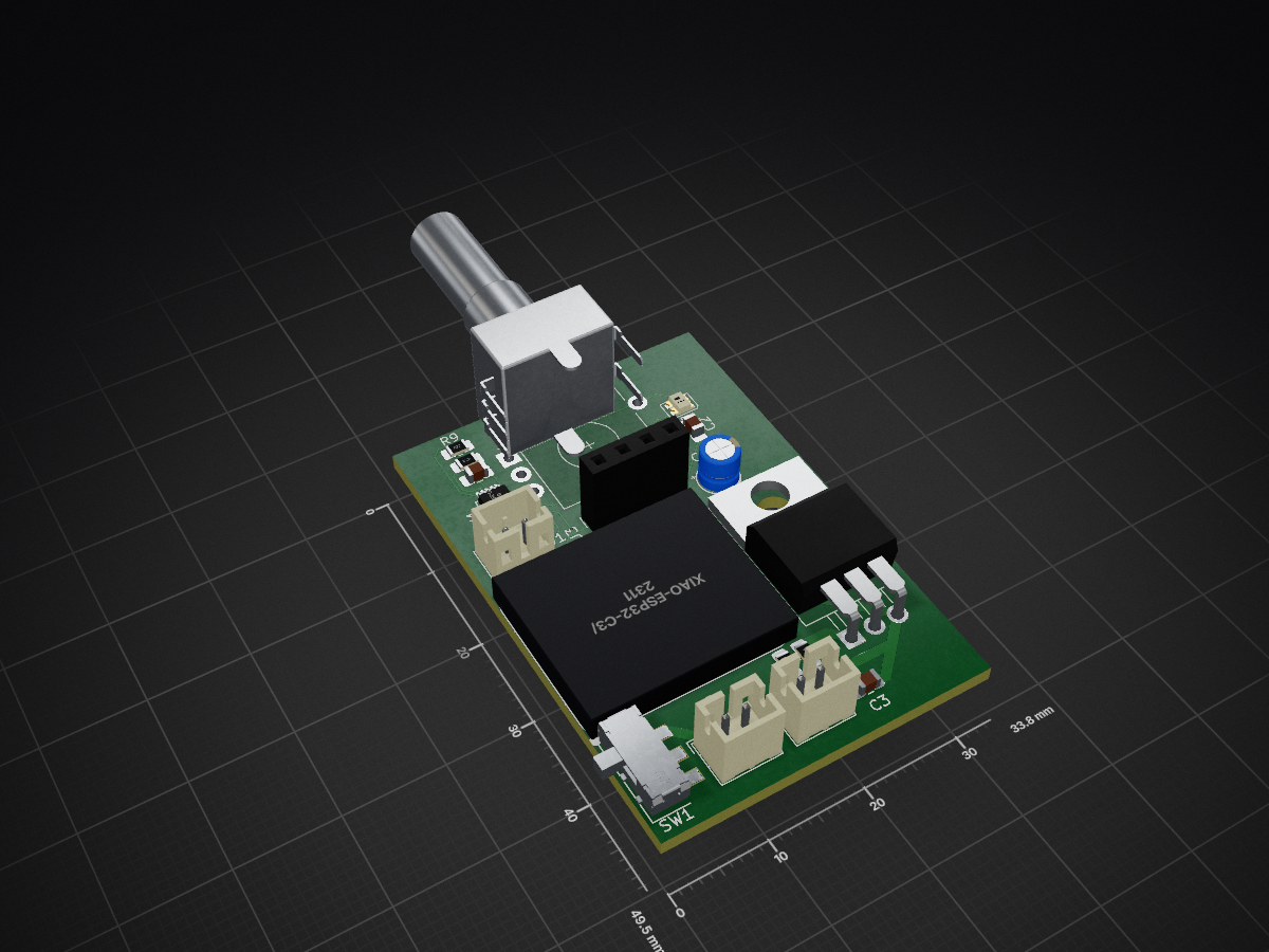
 Adamibus/ESPAtomizer-iOS1
This is a minimal KiCad 6/7 project skeleton. Open ESPAtomizer.kicadpro in KiCad.
EspAtomizerpcbv3rev1 is an open-source printed circuit board by Adamibus, from the Adamibus/ESPAtomizer-iOS repository on GitHub. It is a 2-layer board of 33.8 × 49.5 mm with 21 parts on 29 nets, routed with 150 tracks and 4 vias.
It is built around the ADS1115IDGS, IRLB8721PBF and WS2812B-2020. Its parts include 6 resistors, 4 capacitors, 4 connectors, 2 ICs and 2 diodes. It belongs with the ESP32 and RISC-V boards of this library.


This is a minimal KiCad 6/7 project skeleton. Open ESPAtomizer.kicad_pro in KiCad.
Note: For local firmware build/upload verification and examples, see tools/README.md. It documents
tools/verify_xiao_variants.ps1, a PowerShell helper that builds (and optionally uploads) the firmware for both XIAO ESP32-C3 and XIAO ESP32-C6 environments.
Schematic
ESPAtomizer.kicad_schXIAO:XIAO_ESP32C6_Module (composite symbol) with footprint XIAO:XIAO_ESP32C6_SocketModule (single footprint including both header rows)Transistor_FET:Q_NMOS_GDS) + R3 (100 Ω gate series) + R2 (100 kΩ gate pulldown) + J5 heater terminal (HEATER+ / HEATER−)Rotary_Encoder_Switch) A/B/ENC_SW nets to GPIO0/1/2Board
ESPAtomizer.kicad_pcbPowering from 1S LiPo
Test points & silkscreen
Fabrication
Refer to docs/PCB-PROTOTYPING.md for detailed layout and bring‑up notes.
ESPAtomizer/config.h is the single source of truth for board pin assignments used by the firmware. Keep pin changes centralized there to avoid divergence between schematic/PCB and code.config.h directly. Examples:
platformio.ini under your environment):
build_flags = -DOUTPUT_PIN=5 -DD10_PIN=19arduino-cli compile --fqbn <your_fqbn> -DOUTPUT_PIN=5 -DD10_PIN=19 path/to/ESPAtomizerconfig.h maps the correct physical GPIOs from the PCB; prefer changing config.h or using build flags rather than editing the main sketch.Critical pin-mapping mismatch: The PCB currently routes the MOSFET gate net (MOSFET_GATE) to Pad 1 / GPIO0 on the XIAO footprint, while the schematic/docs state MOSFET_GATE should be driven from GPIO16. GPIO0 is a boot/strapping-related pin on Espressif modules and driving or pulling it during reset can prevent normal boot (puts the chip in download/boot mode). Do not fabricate without resolving this.
Immediate recommendation: Reassign MOSFET_GATE to the non-strapping pin (GPIO16 / Pad 7) to match documentation and avoid boot issues. If you cannot move the net, re-evaluate the pull resistor strategy on GPIO0 (very small chance acceptable only after consulting Espressif strapping rules) — but changing to GPIO16 is the safer, preferred fix.
MOSFET gate & heater current: The BOM warns to verify the MOSFET's RDS(on) at VGS = 3.3 V. Confirm the chosen MOSFET is guaranteed to fully switch at 3.3 V (logic-level device). If not, replace with a MOSFET specified for low RDS(on) at 2.5–3.3 V or add a gate driver.
BAT_ADC (GPIO21) and protection: BAT_ADC is connected to GPIO21 per schematic. Verify GPIO21 supports ADC on the ESP32‑C6 variant used in the XIAO module and ensure a proper resistor divider, input clamp/TVS, and C (10 nF recommended) are present to protect the ADC input from battery voltage.
Power & decoupling: Confirm presence of an LDO/regulator if you expect the module to be powered from BAT directly to 3.3 V. Ensure adequate local decoupling caps placed close to the module's 3V3 pad (C0G/NP0 and bulk electrolytic as needed). I did not find a dedicated LDO footprint in the quick pass; verify whether the XIAO module expects an external 3.3 V supply or provides internal regulation.
RF / antenna keepout: The XIAO module likely contains the RF antenna — keep the placement notes and antenna keepout from PLACEMENT.md enforced. Verify there is no copper or ground pours in the antenna keepout area on the PCB revision.
Assembly / placement notes: Place gate series resistor (R3) and gate pulldown (R2) close to the MOSFET pads as documented. If you move the MOSFET gate net to GPIO16, also update config.h and any firmware references.
Do not release to fabrication yet: Fix the MOSFET_GATE mapping (and optionally verify gate/pull resistor values, MOSFET RDS(on) at 3.3 V, and BAT_ADC clamps) before ordering boards.
MOSFET_GATE from Pad 1 (GPIO0) to Pad 7 (GPIO16), then run ERC and update PCB from schematic.bom-mosfet-alternates.csv or replace with a guaranteed logic-level MOSFET if needed.3V3 rail.If you want, I can prepare the KiCad schematic patch to reassign the MOSFET gate net to Pad 7 (GPIO16) and update config.h accordingly; tell me to proceed and I will make the edits and run another pass of checks.
| Qty | Value | Footprint | References |
|---|---|---|---|
| 3 | 100k | Resistor_SMD:R_0805_2012Metric_Pad1.20x1.40mm_HandSolder | R2, R3, R4 |
| 3 | 100nf | Capacitor_SMD:C_0805_2012Metric_Pad1.18x1.45mm_HandSolder | C1, C2, C3 |
| 2 | 4.7k | Resistor_SMD:R_0805_2012Metric_Pad1.20x1.40mm_HandSolder | R8, R9 |
| 1 | 100Ohm | Resistor_SMD:R_0805_2012Metric_Pad1.20x1.40mm_HandSolder | R1 |
| 1 | 100uf | Capacitor_THT:CP_Radial_D4.0mm_P1.50mm | C5 |
| 1 | ADS1115IDGS | Package_SO:TSSOP-10_3x3mm_P0.5mm | U1 |
| 1 | BATT | Connector_JST:JST_PH_B2B-PH-K_1x02_P2.00mm_Vertical | J2 |
| 1 | Encoder | Rotary_Encoder:RotaryEncoder_Alps_EC11E-Switch_Vertical_H20mm | SW2 |
| 1 | HEAT | Connector_JST:JST_PH_B2B-PH-K_1x02_P2.00mm_Vertical | J4 |
| 1 | IRLB8721PBF | Package_TO_SOT_THT:TO-220F-3_Horizontal_TabDown | Q1 |
| 1 | OLED | Connector_PinSocket_2.54mm:PinSocket_1x04_P2.54mm_Vertical | J3 |
| 1 | SS34 or 1N5819 | Diode_SMD:D_0805_2012Metric_Pad1.15x1.40mm_HandSolder | D2 |
| 1 | SW | footprints:SW_JS102011SAQN | SW1 |
| 1 | THRK | Connector_JST:JST_PH_B2B-PH-K_1x02_P2.00mm_Vertical | J1 |
| 1 | WS2812B-2020 | LED_SMD:LED_WS2812B-2020_PLCC4_2.0x2.0mm | D1 |
| 1 | XIAO-ESP32-C3/C6 | XIAO:XIAOESP32C6_CUSTOM | U3 |
Adamibus/ESPAtomizer-iOS
This is a minimal KiCad 6/7 project skeleton. Open ESPAtomizer.kicadpro in KiCad.

Adamibus/ESPAtomizer-iOS
This is a minimal KiCad 6/7 project skeleton. Open ESPAtomizer.kicadpro in KiCad.

Adamibus/ESPAtomizer-iOS
This is a minimal KiCad 6/7 project skeleton. Open ESPAtomizer.kicadpro in KiCad.

Adamibus/ESPAtomizer-iOS
This is a minimal KiCad 6/7 project skeleton. Open ESPAtomizer.kicadpro in KiCad.


arvindsa/decabox
A compact, intelligent battery management system for 6× Decapo batteries used with cochlear speech processors. This project monitors cell voltage, ambient light, and battery state-of-charge in real-time, with visual…

KoffeinFlummi/rustbucket
Access your car's diagnostics with a BeagleBone Blue and Rust.


stelioskat/esp8266-led-dimmer
Wifi enabled LED strip dimmer that is controlled using MQTT messages.


It measures 33.8 × 49.5 mm and has 2 copper layers, 1.6 mm thick.
21 parts, built around the ADS1115IDGS, IRLB8721PBF and WS2812B-2020. The full list of its parts is on this page, with links to each part's symbol and footprint where PCBKit's library has them.
From the Adamibus/ESPAtomizer-iOS repository on GitHub, at the commit this page was made from: the board is hardware/EspAtomizer-PCB_v3/EspAtomizerpcbv3rev1.kicad_pcb and its schematic hardware/ESPAtomizer_PCB/ESPAtomizer.kicad_sch. PCBKit opens the board in the browser, with nothing to install.
Its repository states no licence, so its author keeps all rights: ask Adamibus before reusing the design.