2 layers630 × 300 mm
 0nonymous/Breadboard-CPU-Computer-System4
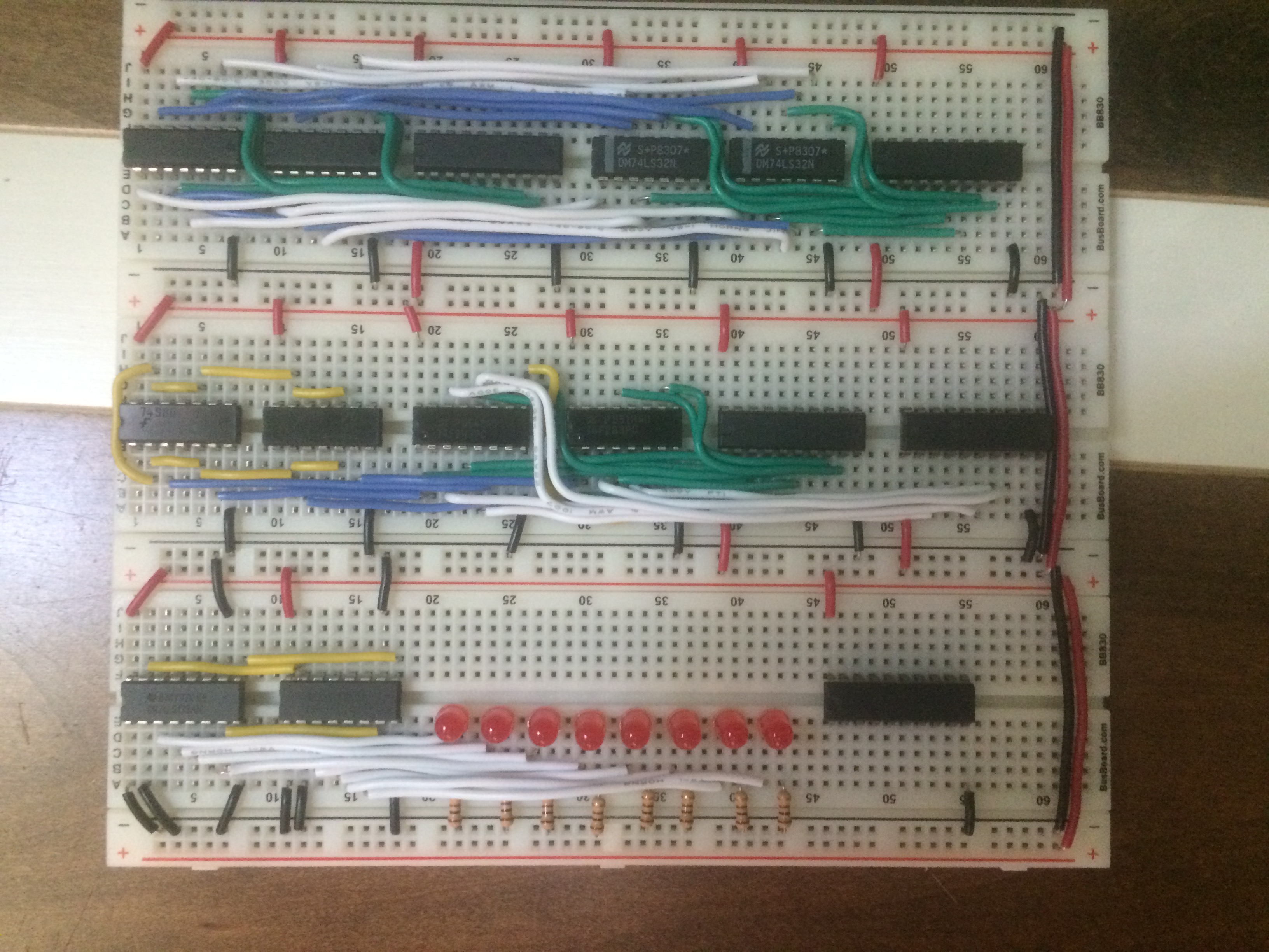
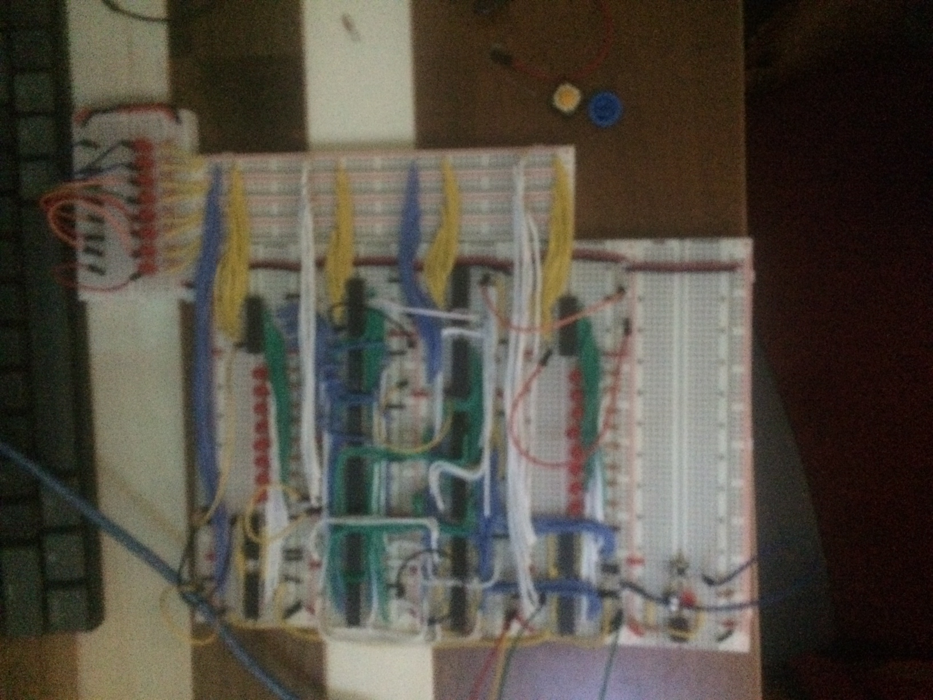
This project is a fully microcoded 8-bit CPU designed from scratch and implemented using 100+ 74LS-series ICs across 40+ breadboards. CURRENTLY REIMPLEMENTING ON FPGA: https://github.com/0nonymous/fpga-cpu
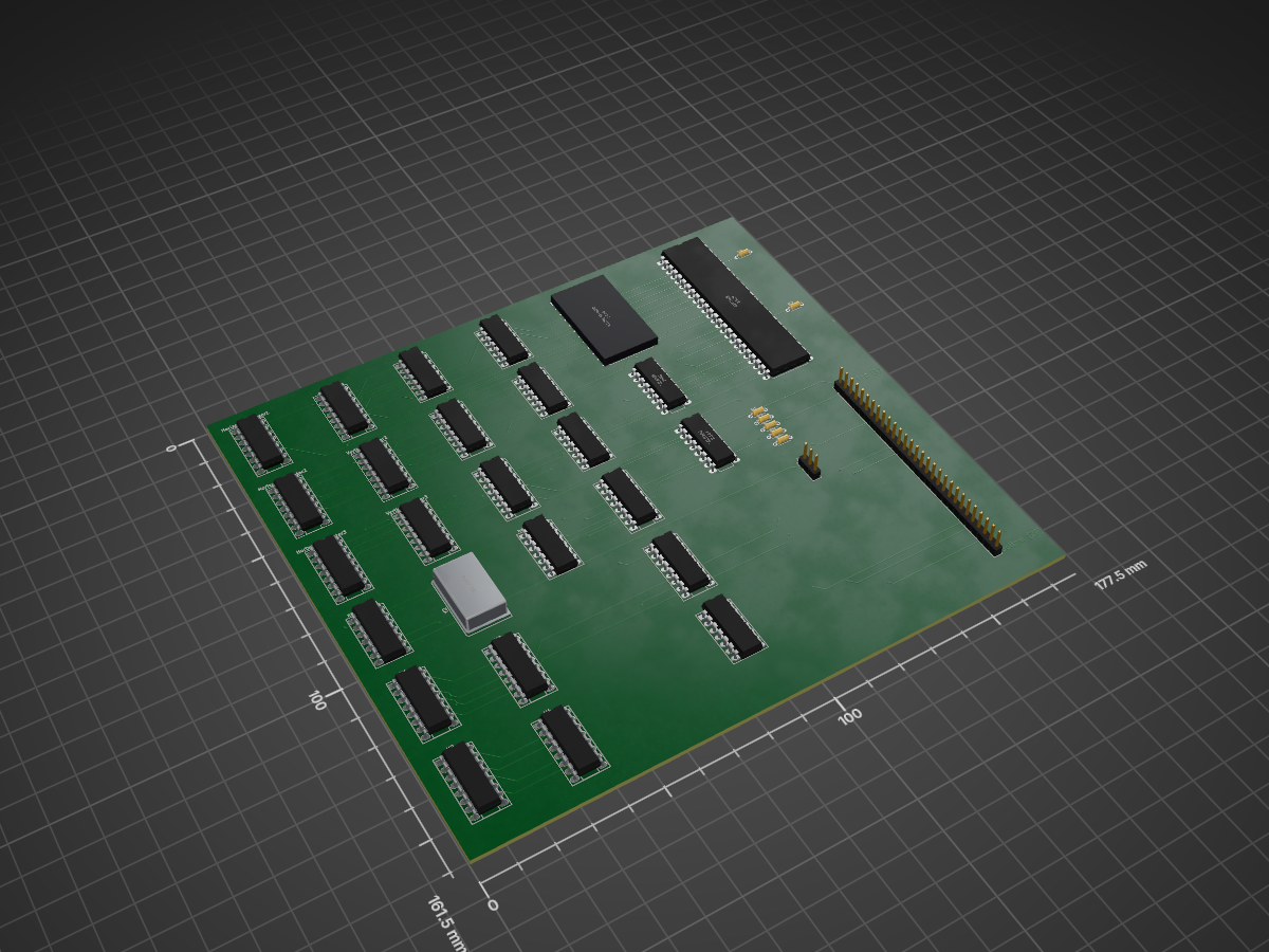
Video circuit is an open-source printed circuit board by 0nonymous, from the 0nonymous/Breadboard-CPU-Computer-System repository on GitHub, published under the MIT licence. It is a 2-layer board of 177.5 × 161.5 mm with 35 parts on 191 nets, routed with 903 tracks and 67 vias.
It is built around the 74LS85DC, 74LS30PC and 74LS04PC, with the 74LS151PC, 74LS32SC and 74LS161DC among its other parts. Its parts include 17 ICs, 7 resistors, 2 connectors and 1 crystal. It belongs with the retro computing and games boards of this library.


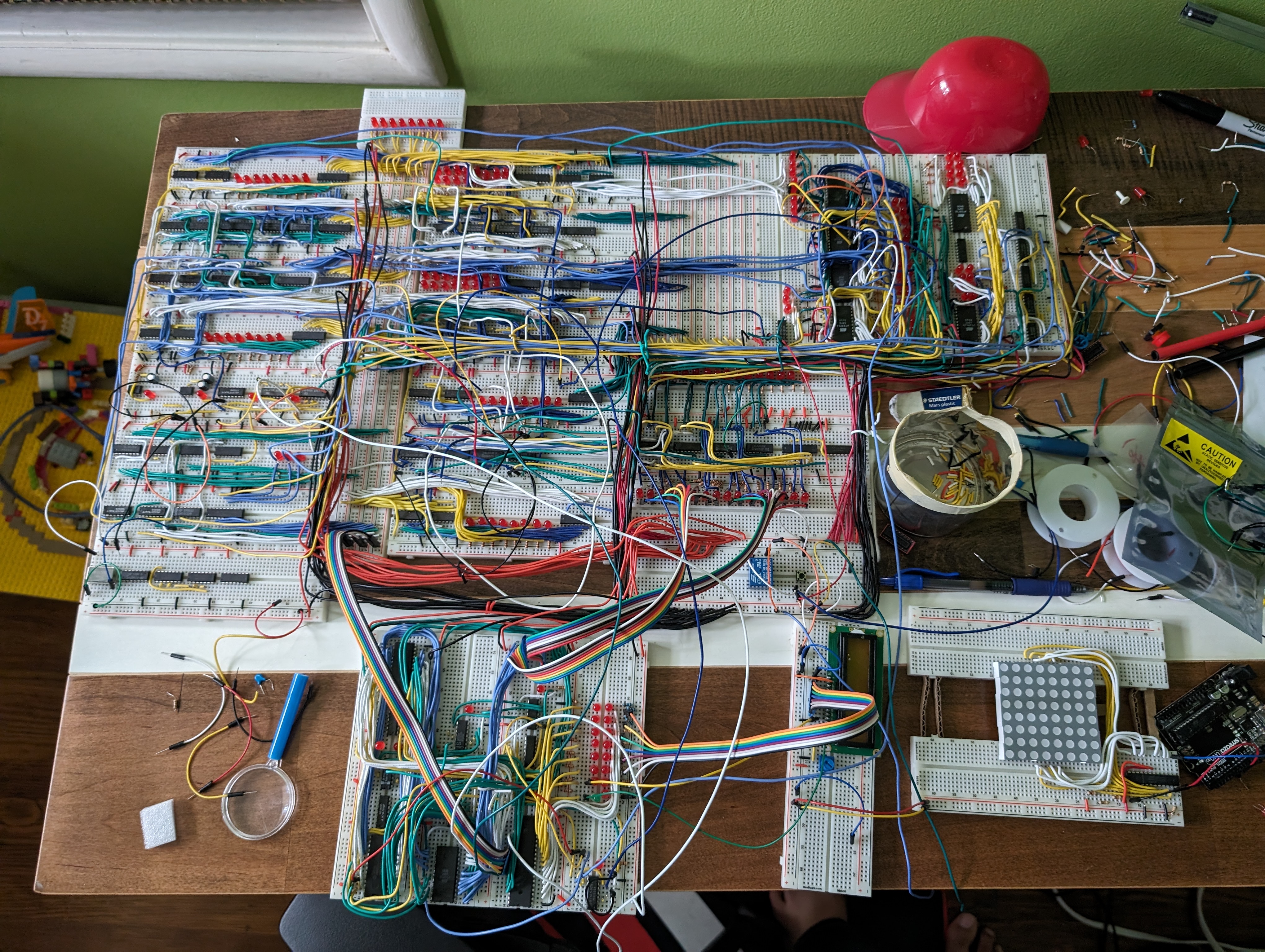
This project is a fully microcoded 8-bit CPU designed from scratch and implemented using 100+ 74LS-series ICs across 40+ breadboards.
The system includes:
This is the third architectural iteration. Earlier versions exposed architectural limitations. The current version runs reliably at approximately ~0.25 MHz.
The assembler uses suffix symbols to indicate addressing modes:
$ = Immediate@ = Absolute# = Indirect (pointer-based)& = Absolute + X offsetExample:
lda $10
lda @2000
lda #3000
lda &4000
inx0x00 lda $
0x01 lda @
0x02 lda #
0x03 lda &
0x04 ldx $
0x05 ldx @
0x06 ldx #
0x07 ldx &
0x08 inx
0x09 dex
0x0A txa
0x0B tax
0x0C add $
0x0D add @
0x0E add #
0x0F add &
0x10 sub $
0x11 sub @
0x12 sub #
0x13 sub &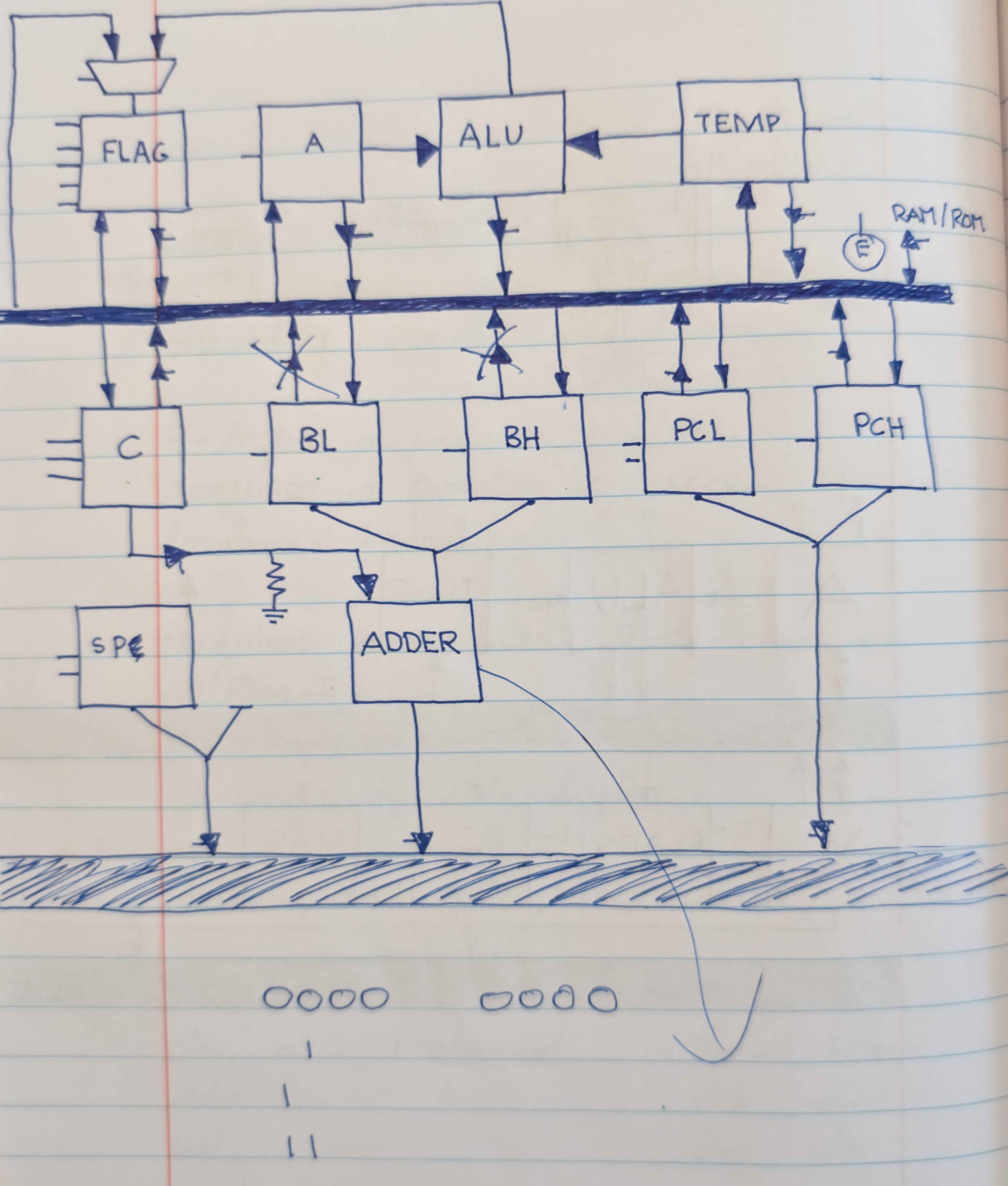
The ALU is implemented using discrete TTL logic:
The CPU uses a horizontal microcode architecture.
The microstep counter increments sequentially and overflows to reset.
Conditional branches do not alter microcode sequencing.
Instead, discrete logic gates PC load signals based on flag conditions (Z, C, S).
Each microinstruction directly drives register enables, ALU operations, bus drivers, PC control, memory read/write, and flag updates.
Total address space: 64KB
Current configuration includes:
Stack resides in a dedicated page and grows downward.
The CPU integrates with a separate VGA driver module.
Features:
The CPU writes character data into shared dual-port memory.
The VGA module independently reads this memory to generate video timing and pixel output.
VGA signal generation approach was inspired by Ben Eater’s methodology and adapted for this architecture.
Custom Python-based programming pipeline:
Two-pass assembler:
Outputs a hex array representation of machine code.
A secondary Python script converts the output into binary format for ROM flashing via XGPro.
Major issue encountered:
Debugging involved:
System runs reliably at approximately ~1 MHz.
Estimated current draw: ~1.2–1.6A under load.
| Qty | Value | Footprint | References |
|---|---|---|---|
| 8 | 74LS85 | Package_DIP:DIP-16_W7.62mm_Socket_LongPads | U1, U2, U3, U4, U6, U7, U11, U12 |
| 7 | R | Resistor_THT:R_Axial_DIN0204_L3.6mm_D1.6mm_P5.08mm_Horizontal | R1, R2, R3, R4, R5, R6, R7 |
| 6 | 74LS161 | Package_DIP:DIP-16_W7.62mm_Socket_LongPads | HorizontalCounter1, HorizontalCounter2, HorizontalCounter3, VerticalCounter1, VerticalCounter2, VerticalCounter3 |
| 2 | 74LS00 | Package_DIP:DIP-14_W7.62mm_Socket_LongPads | nandBoard1, nandBoard2 |
| 2 | 74LS30 | Package_DIP:DIP-14_W7.62mm_Socket_LongPads | U5, U13 |
| 1 | 14, 13, R | Connector_PinHeader_2.54mm:PinHeader_1x03_P2.54mm_Vertical | J1 |
| 1 | 74LS04 | Package_DIP:DIP-14_W7.62mm_Socket_LongPads | U10 |
| 1 | 74LS08 | Package_DIP:DIP-14_W7.62mm_Socket_LongPads | U8 |
| 1 | 74LS151 | Package_DIP:DIP-16_W7.62mm_LongPads | U16 |
| 1 | 74LS283 | Package_DIP:DIP-16_W7.62mm_LongPads | U17 |
| 1 | 74LS32 | Package_DIP:DIP-14_W7.62mm_Socket_LongPads | U9 |
| 1 | AT28C16-15PC | footprints:PDIP24_14P4X32P3_MCH | U15 |
| 1 | CXO_DIP14 | Oscillator:Oscillator_DIP-14 | Y2 |
| 1 | Conn_01x29_Pin | Connector_PinHeader_2.54mm:PinHeader_1x29_P2.54mm_Vertical | J3 |
| 1 | IDT7132 | Package_DIP:DIP-48_W15.24mm_LongPads | U14 |
It measures 177.5 × 161.5 mm and has 2 copper layers, 1.6 mm thick.
35 parts, built around the 74LS85DC, 74LS30PC, 74LS04PC and 74LS151PC. The full list of its parts is on this page, with links to each part's symbol and footprint where PCBKit's library has them.
From the 0nonymous/Breadboard-CPU-Computer-System repository on GitHub, at the commit this page was made from: the board is Test KiCad/video circuit/video circuit.kicad_pcb and its schematic Test KiCad/Test KiCad.kicad_sch. PCBKit opens the board in the browser, with nothing to install.
Its repository publishes it under the MIT licence: you may reuse it on that licence's terms (keep the author's notice, and for a copyleft licence share your changes alike).


electrickery/VIO_MPF_I
Extended firmware for the 6845 based video card for the Microprofessor MPF-I(b)

jimbro1000/DIY-Video
General purpose video system for 8-bit computers using 74LS logic


roberto314/GIMIX_reproduction
Reproducing SS-50 and SS-30 cards and GIMIX Ghost Case and Mainboard
