2 layers110 × 100 mm
ESP32-S3-IO DEVICE
noritama-lab/esp32io-hw
ESP32 ベースの I/O ボードのハードウェア設計をまとめたリポジトリです。 / Hardware designs for an ESP32‑based PLC‑compatible I/O board.
85 parts2
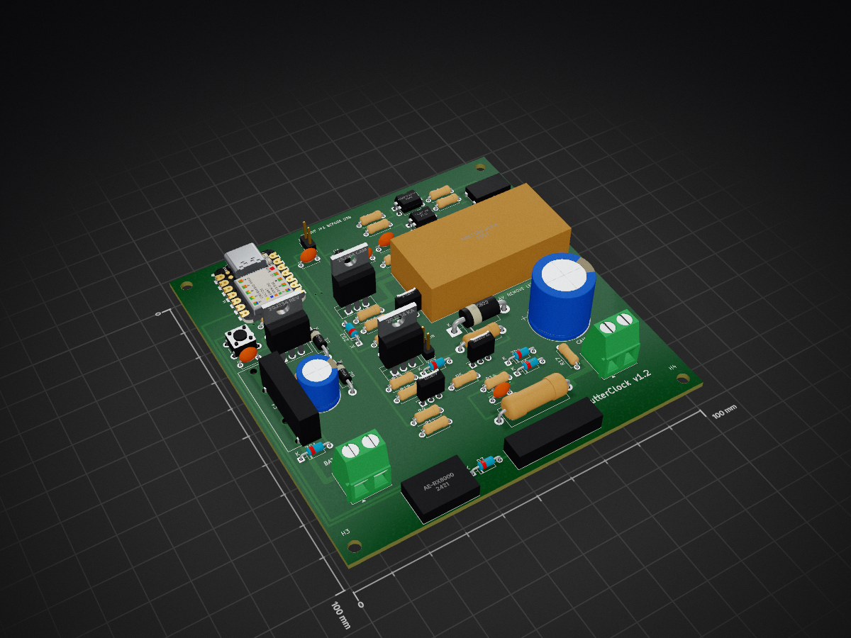
 0kam/ShutterClock
Low-power BLE interval timer for fixed-point Nikon DSLR cameras (XIAO nRF52840, Zephyr, Web Bluetooth)
ShutterClock is an open-source printed circuit board by 0kam, from the 0kam/ShutterClock repository on GitHub. It is a 2-layer board of 100 × 100 mm with 61 parts on 41 nets, routed with 221 tracks and 8 vias.
It is built around the NJW4181U3-33B-TE2, 2SK4017(Q) and P4KE15A, with the CR2032 among its other parts. Its parts include 21 resistors, 7 capacitors, 6 transistors, 5 ICs and 5 diodes. It belongs with the radio and wireless boards and the nRF52 and nRF5x boards of this library.


v1.2 (2026-10-21, not ordered): v1.1 + battery-backed RTC. Board grown to 100 x 100 mm
(mounting holes 93 x 93 mm); a 12 mm strip at the bottom carries U5 Akizuki AE-RX8900
(RX8900CE DTCXO RTC, I2C 0x32 on the XIAO D4 = SDA / D5 = SCL, VDD from 3V3_SYS, FOE tied to
GND so FOUT stays off), BT1 CH243-2032LF vertical CR2032 holder and D7 1N4148 in series
with the cell (the RX8900 has an internal VDD -> VBAT charge path; a CR2032 must not be charged).
SW1 and ZD1 moved 1-2 mm right to make room for the I2C / 3V3 tracks along the left edge.
DRC 0 errors / 0 unconnected. ShutterClock_v1.2_gerbers.zip, render_top.png,
../docs/assembly/placement_top_v1.2.png. Open before ordering: the holder's centre pin is
assumed to be "+" (drawing CH243-0308 does not mark polarity) - check with a cell and a meter on
the real part; if the outer pins are "+", swap BT1 pad nets in generate_board.py.
v1.1 (2026-10-21, not ordered): the three v1.0 errata fixed (C1 polarity nets, U2 hole
pattern 40 x 17.5 mm, F1 clip pins along the fuse axis at 7.0 mm; ZD1 moved 3.5 mm down to make
room). DRC 0 errors / 0 unconnected (40 silk warnings). Gerbers ShutterClock_v1.1_gerbers.zip,
renders render_top.png / render_bottom.png, placement map ../docs/assembly/placement_top_v1.1.png.
Same outline, mounting holes and connector positions as v1.0, so the v1.0 bench results apply.
v1.0 (ordered 2026-10-08, JLCPCB W2026100808086019 / Y14-13437881A, 5 pcs; board #1 assembled
and bench-tested 2026-10-20): ShutterClock_v1.0_gerbers.zip, render_top_v1.0.png /
render_bottom_v1.0.png. Build the remaining v1.0 boards with the workarounds in
../docs/02_assembly.md.
Board: 100 x 88 mm, 2-layer. Bottom layer is a GND pour; most signals on top, the VIN trunk and a few long signals on the bottom.
Mounting: 4x M3 (3.2 mm) holes, centres 3.5 mm from each edge (93 x 81 mm spacing).
Generated by generate_board.py (+ tracks.py) →
ShutterClock.kicad_pcb (KiCad 10). Never hand-edit the .kicad_pcb.
Run: /Applications/KiCad/KiCad.app/Contents/Frameworks/Python.framework/Versions/Current/bin/python3 generate_board.py
then kicad-cli pcb drc --severity-error --severity-warning --format json --output drc.json ShutterClock.kicad_pcb
and python3 drc_report.py. Current state: DRC 0 errors, 0 unconnected (46 warnings: silkscreen overlaps, library-name notes).
Gerbers for JLCPCB (2 layers, 1.6 mm, HASL, defaults): see the version list above. Export: kicad-cli pcb export gerbers --layers F.Cu,B.Cu,F.Paste,B.Paste,F.Silkscreen,B.Silkscreen,F.Mask,B.Mask,Edge_Cuts --subtract-soldermask, kicad-cli pcb export drill --format excellon --excellon-units mm --generate-map --map-format gerberx2, zip the folder. kicad-cli = /Applications/KiCad/KiCad.app/Contents/MacOS/kicad-cli.
Circuit: spec v0.11 §6 (independent review applied). BOM: ../docs/01_parts.md. Assembly guide: ../docs/02_assembly.md (placement map generated by ../docs/assembly/draw_placement.py).
generate_board.py assigns C1 pad 1 (the square
pad, which the KiCad CP_Radial footprint marks "+") to GND and pad 2 to VIN. Electrically the
board is fine; mount C1 with its + lead in the right-hand (round) pad. v1.1: swap the nets
to {"1": "VIN", "2": "GND"} and re-route the two C1 tracks. C3 is correct (pad 1 = CAM_P).fp_buck() pads at ±20.0 / ±8.75 mm.fp_fuseclips() (pairs 6.7 mm apart across the axis). v1.0 boards: cut one pin per clip and
solder the other into one hole (keep the outer pin on one clip and the inner pin on the other
so the clip spacing stays 18 mm), or put an inline fuse holder in the battery + lead and bridge
the F1 holes. v1.1: rotate the footprint; pin pitch along the axis still to be measured.| XIAO pin | Net | Function |
|---|---|---|
| A0 (D0) | ADC_NODE | Battery voltage: VIN × 100k/(1M+100k) (ungated divider, 100 nF). Reading × 11 |
| A1 (D1) | A1_NODE | Camera current: 0.1 Ω low-side shunt in the camera return (CAM_N), 10 kΩ + 100 nF. 1 A = 0.1 V |
| D2 | AF_DRV | PC817 U4 (AF / half-press) via 1 kΩ. High = pressed |
| D7 | CAM_EN | Camera supply: Q3 → Q2 → MBC2596-01 (9.4 V) → 1N5822 → CAM_P. High = on |
| D8 | SHUT_DRV | PC817 U3 (SHUTTER / full-press) via 1 kΩ. High = pressed |
| D9 | BTN | Test-shot / BLE button SW1 to GND (enable the internal pull-up) |
| D10 | KA_EN | Keep-alive path: Q6 → Q5 → 10 Ω → Q7 follower (≈ 7.3–8.5 V) → CAM_P. High = on |
| 3V3 | 3V3_SYS | From U1 (NJW4181U3-33B) through JP1 |
| GND | GND | |
| D4 / D5 | SDA / SCL | v1.2: RX8900 RTC module U5 (i2c1). Unused on v1.0 / v1.1 |
| D3, D6, 5V | — | unused |
Rules: never drive CAM_EN and KA_EN so that the camera is released on the keep-alive path; enter keep-alive only from CAM_EN = on; drop to CAM_EN = on if A1 shows > 50 mA during keep-alive; low-battery cutoff 11.5 V.
"REMOVE JP1 BEFORE USB", "U2: SET 9.4V, REMOVE LED", "JP2=ALWAYS ON", battery and camera polarity, diode cathodes marked "K".
| Qty | Value | Footprint | References |
|---|---|---|---|
| 5 | 100k | R_Axial_DIN0207_L6.3mm_D2.5mm_P7.62mm_Horizontal | R2, R10, R11, R12, R13 |
| 4 | 1k | R_Axial_DIN0207_L6.3mm_D2.5mm_P7.62mm_Horizontal | R6, R7, R8, R9 |
| 4 | M3 | MountingHole_3.2mm_M3 | H1, H2, H3, H4 |
| 3 | 0.1u | C_Disc_D5.0mm_W2.5mm_P5.00mm | C6, C7, C8 |
| 3 | 100 | R_Axial_DIN0207_L6.3mm_D2.5mm_P7.62mm_Horizontal | R4, R20, R21 |
| 3 | 15V | D_DO-35_SOD27_P7.62mm_Horizontal | ZD1, ZD2, ZD3 |
| 3 | 1M | R_Axial_DIN0207_L6.3mm_D2.5mm_P7.62mm_Horizontal | R1, R15, R17 |
| 2 | 1N4148 | D_DO-35_SOD27_P7.62mm_Horizontal | D6, D7 |
| 2 | 2SK4017 | TO-251-3_Vertical | Q3, Q6 |
| 2 | 33k | R_Axial_DIN0207_L6.3mm_D2.5mm_P7.62mm_Horizontal | R16, R18 |
| 2 | P4KE15A | D_DO-41_SOD81_P10.16mm_Horizontal | D1, D2 |
| 1 | 0.1R 3W | R_Axial_DIN0617_L17.0mm_D6.0mm_P20.32mm_Horizontal | R3 |
| 1 | 100u/50V | CP_Radial_D10.0mm_P5.00mm | C1 |
| 1 | 10R 1W | R_Axial_DIN0411_L9.9mm_D3.6mm_P12.70mm_Horizontal | R19 |
| 1 | 10k | R_Axial_DIN0207_L6.3mm_D2.5mm_P7.62mm_Horizontal | R14 |
| 1 | 10u | C_Disc_D5.0mm_W2.5mm_P5.00mm | C2 |
| 1 | 1N5822 | D_DO-201AD_P15.24mm_Horizontal | D4 |
| 1 | 2.2u | C_Disc_D5.0mm_W2.5mm_P5.00mm | C4 |
| 1 | 2SJ334 CAM | TO-220-3_Vertical | Q2 |
| 1 | 2SJ334 KA | TO-220-3_Vertical | Q5 |
| 1 | 2SJ334 REV | TO-220-3_Vertical | Q1 |
| 1 | 2SK4017 KA | TO-251-3_Vertical | Q7 |
| 1 | 3.5mm RELEASE | ShutterClock:MJ-8435 | J3 |
| 1 | 4700u/16V | CP_Radial_D16.0mm_P7.50mm | C3 |
| 1 | 47k | R_Axial_DIN0207_L6.3mm_D2.5mm_P7.62mm_Horizontal | R5 |
| 1 | 5A | ShutterClock:FUC-03A_x2_5x20 | F1 |
| 1 | 9.1V | D_DO-35_SOD27_P7.62mm_Horizontal | ZD4 |
| 1 | AE-RX8900 | ShutterClock:AE-RX8900 | U5 |
| 1 | BATTERY 12V | TerminalBlock_Phoenix_MKDS-1,5-2-5.08_1x02_P5.08mm_Horizontal | J1 |
| 1 | CAMERA EP-5B | TerminalBlock_Phoenix_MKDS-1,5-2-5.08_1x02_P5.08mm_Horizontal | J2 |
| 1 | CR2032 | ShutterClock:CH243-2032LF | BT1 |
| 1 | JP1 3V3 | PinHeader_1x02_P2.54mm_Vertical | JP1 |
| 1 | JP2 ALWAYS ON | PinHeader_1x02_P2.54mm_Vertical | JP2 |
| 1 | MBC2596-01 9.4V | ShutterClock:MBC2596-01 | U2 |
| 1 | NJW4181U3-33B | SOT-89-3 | U1 |
| 1 | PC817 AF | DIP-4_W7.62mm | U4 |
| 1 | PC817 SHUTTER | DIP-4_W7.62mm | U3 |
| 1 | TEST | SW_PUSH_6mm | SW1 |
| 1 | XIAO nRF52840 | XIAO-nRF52840-DIP | A1 |
It measures 100 × 100 mm and has 2 copper layers, 1.6 mm thick.
61 parts, built around the NJW4181U3-33B-TE2, 2SK4017(Q), P4KE15A and CR2032. The full list of its parts is on this page, with links to each part's symbol and footprint where PCBKit's library has them.
From the 0kam/ShutterClock repository on GitHub, at the commit this page was made from: the board is pcb/ShutterClock.kicad_pcb. PCBKit opens the board in the browser, with nothing to install.
Its repository states no licence, so its author keeps all rights: ask 0kam before reusing the design.
noritama-lab/esp32io-hw
ESP32 ベースの I/O ボードのハードウェア設計をまとめたリポジトリです。 / Hardware designs for an ESP32‑based PLC‑compatible I/O board.


tokai-student-rocket-project/H-62-Avionics
H-62搭載計器 すばる1.3 | 2025年度 夏季 能代 NOGO


Dudestin/tinyEtherDeveloper
Inexpensive FPGA board-based Ethernet evaluation board project. Consists mostly of DIP components and uses Tang PriMER. It can be built for about $50.

