2 layers85 × 115 mm
OSO BOOK C1
joeycastillo/The-Open-Book
For details on how to build, test and use Open Book, I've made documentation available here.
38 parts8.1kCC-BY-SA-4.0

 zoriya/abyss14
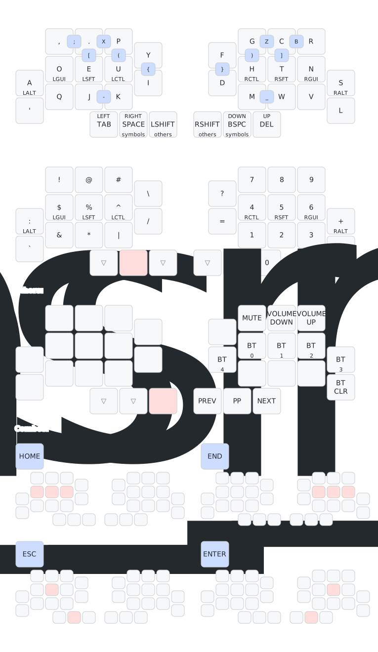
A weird split 32 key keyboard
Abyss is an open-source printed circuit board by zoriya, from the zoriya/abyss repository on GitHub. It is a 2-layer board of 106.5 × 91.8 mm with 38 parts on 31 nets, routed with 683 tracks and 35 vias.
Its parts include 16 diodes and 16 switches. It belongs with the keyboards and input boards of this library.
A 32 key split keyboard with a low pinky column.
| Count | Part name | Size/Remark |
|---|---|---|
| 2x | Seeed Xiao nRF54L15 - mcu | |
| 2x | 1208YD - reset button | 6x6x7mm |
| 2x | 401030 Li-Po Battery | 4x10x30mm |
| 2x | SM02B-SRSS-TB - battery connector | |
| 32x | choc switch | i use sunsets |
| 30x | 1u choc keycaps | i use pom |
| 2x | 1.5u choc keycaps | i use pom |
| 32x | hotswap chock sockets | |
| 32x | diodes | |
| 16x | magnets | 20x8x1.5mm |
| 4x | m2 screws | 4/6/8mm |
| 4x | m2 standoff | <5mm wide, 6mm height |
Case dimensions:
Transport case dimesions:
| Qty | Value | Footprint | References |
|---|---|---|---|
| 16 | ComboDiode | D1, D2, D3, D4, D5, D6, D7, D8, D9, D10, D11, D12, D13, D14, D15, D16 | |
| 16 | PG1350 | S1, S2, S3, S4, S5, S6, S7, S8, S9, S10, S11, S12, S13, S14, S15, S16 |
The 32 most common of 38 parts.
It measures 106.5 × 91.8 mm and has 2 copper layers, 1.6 mm thick.
38 parts. The full list of its parts is on this page, with links to each part's symbol and footprint where PCBKit's library has them.
From the zoriya/abyss repository on GitHub, at the commit this page was made from: the board is pcb/abyss.kicad_pcb and its schematic pcb/abyss.kicad_sch. PCBKit opens the board in the browser, with nothing to install.
Its repository states no licence, so its author keeps all rights: ask zoriya before reusing the design.
joeycastillo/The-Open-Book
For details on how to build, test and use Open Book, I've made documentation available here.


hackclub/OnBoard
💡 Join 1,000 teenagers and make your first PCB with a $100 grant!


Ardumower/ardumower
Develop an open source robotic lawn mower (HW+SW reference platform)

CRImier/MyKiCad
My KiCad boards. Can't be bothered uploading individually anymore, so here you go.

