2 layers38.1 × 20.3 mm

 yutotnh/USB_Type-A_to_DIP
USB Type-A ををDIPで使えるようにする基板
USB Type A to DIP fin is an open-source printed circuit board by yutotnh, from the yutotnh/USB_Type-A_to_DIP repository on GitHub, published under the MIT licence. It is a 2-layer board of 76.2 × 81.3 mm with 32 parts on 4 nets, routed with 88 tracks and 0 vias.
USB Type-A ををDIPで使えるようにする基板
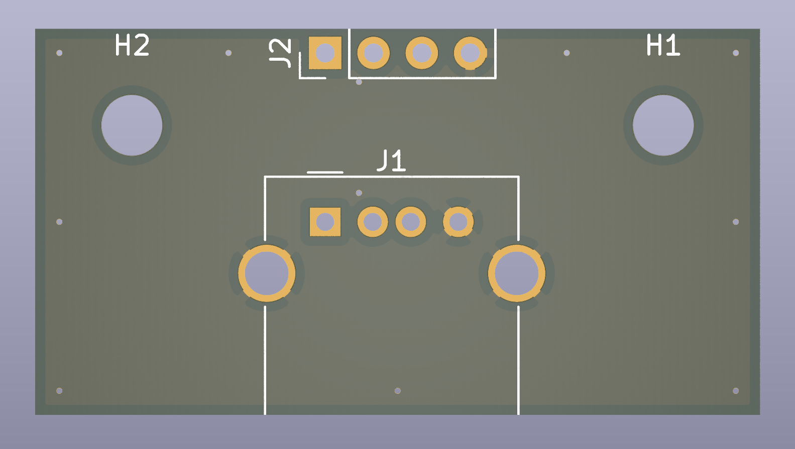
| Qty | Value | Footprint | References |
|---|---|---|---|
| 16 | MountingHole | MountingHole:MountingHole_3.2mm_M3 | H1, H1, H1, H1, H1, H1, H1, H1, H2, H2, H2, H2, H2, H2, H2, H2 |
| 8 | Conn_01x04 | Connector_PinHeader_2.54mm:PinHeader_1x04_P2.54mm_Vertical | J2, J2, J2, J2, J2, J2, J2, J2 |
| 8 | USB_A | Connector_USB:USB_A_Molex_67643_Horizontal | J1, J1, J1, J1, J1, J1, J1, J1 |

hoglet67/RGBtoHDMI
Bare-metal Raspberry Pi project that provides pixel-perfect sampling of Retro Computer RGB/YUV video and conversion to HDMI

hackclub/OnBoard
💡 Join 1,000 teenagers and make your first PCB with a $100 grant!


octosavvi/ESPKey
Wiegand data logger, replay device and micro door-controller

zmaker/arduino_cookbook
gli sketch del nuovo progetto Arduino Cookbook e dei video di YouTube

murexrobotics/electrical
Highly integrated electronics design and printed circuit boards (PCBs) for the MATE ROV Competition. Attempt the impossible.

swharden/AVR-projects
A collection of standalone AVR projects written in C

hardenedlinux/cheap-pcb
Cheap PCB: Better understanding the current status of hardware supply chain
It measures 76.2 × 81.3 mm and has 2 copper layers, 1.6 mm thick.
32 parts. The full list of its parts is on this page, with links to each part's symbol and footprint where PCBKit's library has them.
From the yutotnh/USB_Type-A_to_DIP repository on GitHub, at the commit this page was made from: the board is USB_Type-A_to_DIP_fin.kicad_pcb. PCBKit opens the board in the browser, with nothing to install.
Its repository publishes it under the MIT licence: you may reuse it on that licence's terms (keep the author's notice, and for a copyleft licence share your changes alike).